
The Mini Small Outline Package (MSOP) is a miniaturized version of the small outline integrated circuit packaging format for integrated circuits.
The Mini Small Outline Package (MSOP) is a miniaturized version of the small outline integrated circuit packaging format for integrated circuits.
Many integrated circuits are available in the MSOP form factor. They are suited for space-limited applications requiring 1 mm or less mounted height and are commonly used in disk drives, video/audio and consumer electronics. [1]
The size of the Mini Small Outline Package is only 3mm × 3mm for the 8 and 10 pin versions [1] and 3mm × 4mm for the 12 and 16 pin version. [2] [3] The small package offers a small footprint, short wires for improved electrical connections, and good moisture reliability. [1] Some versions have an exposed pad on the bottom side. The exposed pad will be soldered on the PCB to transfer heat from the package to the PCB. [2] [1]
| Part number | Pins | Body width (mm) | Body length (mm) | Lead pitch (mm) |
|---|---|---|---|---|
| MSOP8 | 8 | 3 | 3 | 0.65 |
| MSOP10 | 10 | 3 | 3 | 0.5 |
| MSOP12 | 12 | 3 | 4 | 0.65 |
| MSOP16 | 16 | 3 | 4 | 0.5 |

In microelectronics, a dual in-line package is an electronic component package with a rectangular housing and two parallel rows of electrical connecting pins. The package may be through-hole mounted to a printed circuit board (PCB) or inserted in a socket. The dual-inline format was invented by Don Forbes, Rex Rice and Bryant Rogers at Fairchild R&D in 1964, when the restricted number of leads available on circular transistor-style packages became a limitation in the use of integrated circuits. Increasingly complex circuits required more signal and power supply leads ; eventually microprocessors and similar complex devices required more leads than could be put on a DIP package, leading to development of higher-density chip carriers. Furthermore, square and rectangular packages made it easier to route printed-circuit traces beneath the packages.

A printed circuit board (PCB), also called printed wiring board (PWB), is a medium used to connect or "wire" components to one another in a circuit. It takes the form of a laminated sandwich structure of conductive and insulating layers: each of the conductive layers is designed with a pattern of traces, planes and other features etched from one or more sheet layers of copper laminated onto and/or between sheet layers of a non-conductive substrate. Electrical components may be fixed to conductive pads on the outer layers in the shape designed to accept the component's terminals, generally by means of soldering, to both electrically connect and mechanically fasten them to it. Another manufacturing process adds vias, plated-through holes that allow interconnections between layers.

A ball grid array (BGA) is a type of surface-mount packaging used for integrated circuits. BGA packages are used to permanently mount devices such as microprocessors. A BGA can provide more interconnection pins than can be put on a dual in-line or flat package. The whole bottom surface of the device can be used, instead of just the perimeter. The traces connecting the package's leads to the wires or balls which connect the die to package are also on average shorter than with a perimeter-only type, leading to better performance at high speeds.

Surface-mount technology (SMT), originally called planar mounting, is a method in which the electrical components are mounted directly onto the surface of a printed circuit board (PCB). An electrical component mounted in this manner is referred to as a surface-mount device (SMD). In industry, this approach has largely replaced the through-hole technology construction method of fitting components, in large part because SMT allows for increased manufacturing automation which reduces cost and improves quality. It also allows for more components to fit on a given area of substrate. Both technologies can be used on the same board, with the through-hole technology often used for components not suitable for surface mounting such as large transformers and heat-sinked power semiconductors.

Flip chip, also known as controlled collapse chip connection or its abbreviation, C4, is a method for interconnecting dies such as semiconductor devices, IC chips, integrated passive devices and microelectromechanical systems (MEMS), to external circuitry with solder bumps that have been deposited onto the chip pads. The technique was developed by General Electric's Light Military Electronics Department, Utica, New York. The solder bumps are deposited on the chip pads on the top side of the wafer during the final wafer processing step. In order to mount the chip to external circuitry, it is flipped over so that its top side faces down, and aligned so that its pads align with matching pads on the external circuit, and then the solder is reflowed to complete the interconnect. This is in contrast to wire bonding, in which the chip is mounted upright and fine wires are welded onto the chip pads and lead frame contacts to interconnect the chip pads to external circuitry.

Integrated circuit packaging is the final stage of semiconductor device fabrication, in which the die is encapsulated in a supporting case that prevents physical damage and corrosion. The case, known as a "package", supports the electrical contacts which connect the device to a circuit board.
A quad flat package (QFP) is a surface-mounted integrated circuit package with "gull wing" leads extending from each of the four sides. Socketing such packages is rare and through-hole mounting is not possible. Versions ranging from 32 to 304 pins with a pitch ranging from 0.4 to 1.0 mm are common. Other special variants include low-profile QFP (LQFP) and thin QFP (TQFP).

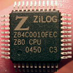
The Zilog Z8 is a microcontroller architecture, originally introduced in 1979, which today also includes the Z8 Encore!, eZ8 Encore!, eZ8 Encore! XP, and eZ8 Encore! MC families.

Thin small outline package (TSOP) is a type of surface mount IC package. They are very low-profile and have tight lead spacing.

TARGET 3001! is a CAD computer program for EDA and PCB design, developed by Ing.-Büro Friedrich in Germany. It supports the design of electronic schematics, PCBs, and device front panels. It runs under Windows and is available in English, German and French.

A small outline integrated circuit (SOIC) is a surface-mounted integrated circuit (IC) package which occupies an area about 30–50% less than an equivalent dual in-line package (DIP), with a typical thickness being 70% less. They are generally available in the same pin-outs as their counterpart DIP ICs. The convention for naming the package is SOIC or SO followed by the number of pins. For example, a 14-pin 4011 would be housed in an SOIC-14 or SO-14 package.

Flat no-leads packages such as quad-flat no-leads (QFN) and dual-flat no-leads (DFN) physically and electrically connect integrated circuits to printed circuit boards. Flat no-leads, also known as micro leadframe (MLF) and SON, is a surface-mount technology, one of several package technologies that connect ICs to the surfaces of PCBs without through-holes. Flat no-lead is a near chip scale plastic encapsulated package made with a planar copper lead frame substrate. Perimeter lands on the package bottom provide electrical connections to the PCB. Flat no-lead packages usually, but not always, include an exposed thermally conductive pad to improve heat transfer out of the IC. Heat transfer can be further facilitated by metal vias in the thermal pad. The QFN package is similar to the quad-flat package (QFP), and a ball grid array (BGA).

A probe card is used in automated integrated circuit testing. It is an interface between an electronic test system and a semiconductor wafer.

In electronics, TO-3 is a designation for a standardized metal semiconductor package used for power semiconductors, including transistors, silicon controlled rectifiers, and, integrated circuits. TO stands for "Transistor Outline" and relates to a series of technical drawings produced by JEDEC.
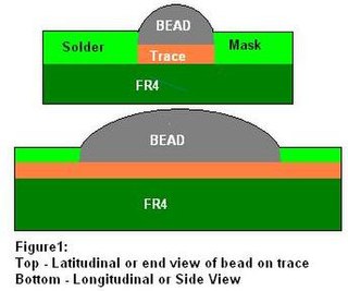
Bead probe technology (BPT) is technique used to provide electrical access to printed circuit board (PCB) circuitry for performing in-circuit testing (ICT). It makes use of small beads of solder placed onto the board's traces to allow measuring and controlling of the signals using a test probe. This permits test access to boards on which standard ICT test pads are not feasible due to space constraints.

DipTrace is a proprietary software suite for electronic design automation (EDA) used for electronic schematic capture and printed circuit board layouts. DipTrace has four applications: schematic capture editor, PCB layout editor with built-in shape-based autorouter and 3D preview, component editor, and pattern editor.

In microelectronics, a quad in-line package, is an electronic component package with a rectangular housing and four parallel rows of electrical connecting pins. The package may be through-hole mounted to a printed circuit board (PCB) or inserted in a socket. Rockwell used a QIP with 42 leads formed into staggered rows for their PPS-4 microprocessor family introduced in 1973, and other microprocessors and microcontrollers, some with higher lead counts, through the early 1990s.
The NEC μCOM series is a series of microprocessors and microcontrollers manufactured by NEC in the 1970s and 1980s. The initial entries in the series were custom-designed 4 and 16-bit designs, but later models in the series were mostly based on the Intel 8080 and Zilog Z80 8-bit designs, and later, the Intel 8086 16-bit design. Most of the line was replaced in 1984 by the NEC V20, an Intel 8088 clone.

The Thin Shrink Small Outline Package (TSSOP) is a rectangular surface mount plastic integrated circuit (IC) package with gull-wing leads.