An integrated circuit or monolithic integrated circuit is a set of electronic circuits on one small flat piece of semiconductor material, usually silicon. Large numbers of miniaturized transistors and other electronic components are integrated together on the chip. This results in circuits that are orders of magnitude smaller, faster, and less expensive than those constructed of discrete components, allowing a large transistor count. The IC's mass production capability, reliability, and building-block approach to integrated circuit design have ensured the rapid adoption of standardized ICs in place of designs using discrete transistors. ICs are now used in virtually all electronic equipment and have revolutionized the world of electronics. Computers, mobile phones and other home appliances are now inextricable parts of the structure of modern societies, made possible by the small size and low cost of ICs such as modern computer processors and microcontrollers.

In microelectronics, a dual in-line package, is an electronic component package with a rectangular housing and two parallel rows of electrical connecting pins. The package may be through-hole mounted to a printed circuit board (PCB) or inserted in a socket. The dual-inline format was invented by Don Forbes, Rex Rice and Bryant Rogers at Fairchild R&D in 1964, when the restricted number of leads available on circular transistor-style packages became a limitation in the use of integrated circuits. Increasingly complex circuits required more signal and power supply leads ; eventually microprocessors and similar complex devices required more leads than could be put on a DIP package, leading to development of higher-density chip carriers. Furthermore, square and rectangular packages made it easier to route printed-circuit traces beneath the packages.

In computing, PC Card is a configuration for computer parallel communication peripheral interface, designed for laptop computers. Originally introduced as PCMCIA, the PC Card standard as well as its successors like CardBus were defined and developed by the Personal Computer Memory Card International Association (PCMCIA).

A ball grid array (BGA) is a type of surface-mount packaging used for integrated circuits. BGA packages are used to permanently mount devices such as microprocessors. A BGA can provide more interconnection pins than can be put on a dual in-line or flat package. The whole bottom surface of the device can be used, instead of just the perimeter. The traces connecting the package's leads to the wires or balls which connect the die to package are also on average shorter than with a perimeter-only type, leading to better performance at high speeds.

The zig-zag in-line package (ZIP) is a packaging technology for integrated circuits. It was intended as a replacement for dual in-line packaging. A ZIP is an integrated circuit encapsulated in a slab of plastic with 16, 20, 28 or 40 pins, measuring about 3 mm x 30 mm x 10 mm. The package's pins protrude in two rows from one of the long edges. The two rows are staggered by 1.27 mm (0.05"), giving them a zig-zag appearance, and allowing them to be spaced more closely than a rectangular grid would allow. The pins are inserted into holes in a printed circuit board, with the packages standing at right-angles to the board, allowing them to be placed closer together than DIPs of the same size. ZIPs have now been superseded by surface-mount packages such as the thin small-outline packages (TSOPs), but are still in use. The quad in-line package uses a similar staggered semiconductor package design.

In electronics manufacturing, integrated circuit packaging is the final stage of semiconductor device fabrication, in which the block of semiconductor material is encapsulated in a supporting case that prevents physical damage and corrosion. The case, known as a "package", supports the electrical contacts which connect the device to a circuit board.

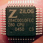
A quad flat package (QFP) is a surface-mounted integrated circuit package with "gull wing" leads extending from each of the four sides. Socketing such packages is rare and through-hole mounting is not possible. Versions ranging from 32 to 304 pins with a pitch ranging from 0.4 to 1.0 mm are common. Other special variants include low-profile QFP (LQFP) and thin QFP (TQFP).

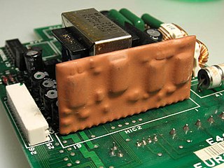
A hybrid integrated circuit (HIC), hybrid microcircuit, hybrid circuit or simply hybrid is a miniaturized electronic circuit constructed of individual devices, such as semiconductor devices and passive components, bonded to a substrate or printed circuit board (PCB). A PCB having components on a Printed Wiring Board (PWB) is not considered a true hybrid circuit according to the definition of MIL-PRF-38534.

A small outline integrated circuit (SOIC) is a surface-mounted integrated circuit (IC) package which occupies an area about 30–50% less than an equivalent dual in-line package (DIP), with a typical thickness being 70% less. They are generally available in the same pin-outs as their counterpart DIP ICs. The convention for naming the package is SOIC or SO followed by the number of pins. For example, a 14-pin 4011 would be housed in an SOIC-14 or SO-14 package.

A multi-chip module (MCM) is generically an electronic assembly where multiple integrated circuits, semiconductor dies and/or other discrete components are integrated, usually onto a unifying substrate, so that in use it can be treated as if it were a larger IC. Other terms for MCM packaging include "heterogeneous integration" or "hybrid integrated circuit". The advantage of using MCM packaging is it allows a manufacturer to use multiple components for modularity and/or to improve yields over a conventional monolithic IC approach.

A system in a package (SiP) or system-in-package is a number of integrated circuits (ICs) enclosed in one chip carrier package or encompassing an IC package substrate that may include passive components and perform the functions of an entire system. The ICs may be stacked using package on package, placed side by side, and/or embedded in the substrate. The SiP performs all or most of the functions of an electronic system, and is typically used when designing components for mobile phones, digital music players, etc. Dies containing integrated circuits may be stacked vertically on a substrate. They are internally connected by fine wires that are bonded to the package. Alternatively, with a flip chip technology, solder bumps are used to join stacked chips together. SiPs are like systems on a chip (SoCs) but less tightly integrated and not on a single semiconductor die.

Flat no-leads packages such as quad-flat no-leads (QFN) and dual-flat no-leads (DFN) physically and electrically connect integrated circuits to printed circuit boards. Flat no-leads, also known as micro leadframe (MLF) and SON, is a surface-mount technology, one of several package technologies that connect ICs to the surfaces of PCBs without through-holes. Flat no-lead is a near chip scale plastic encapsulated package made with a planar copper lead frame substrate. Perimeter lands on the package bottom provide electrical connections to the PCB. Flat no-lead packages usually, but not always, include an exposed thermally conductive pad to improve heat transfer out of the IC. Heat transfer can be further facilitated by metal vias in the thermal pad. The QFN package is similar to the quad-flat package (QFP), and a ball grid array (BGA).

In computing, a memory module or RAM stick is a printed circuit board on which memory integrated circuits are mounted. Memory modules permit easy installation and replacement in electronic systems, especially computers such as personal computers, workstations, and servers. The first memory modules were proprietary designs that were specific to a model of computer from a specific manufacturer. Later, memory modules were standardized by organizations such as JEDEC and could be used in any system designed to use them.
Flashrom is a software utility published under an open source license that can detect, read, verify, erase, or write EEPROMs using interfaces such as the Low Pin Count (LPC), FWH, parallel, and Serial Peripheral Interface (SPI). It can be used to flash firmware images such as BIOS or coreboot, or to backup existing firmware.
A QUADRAC is a special type of thyristor which combines a DIAC and a TRIAC in a single package. The DIAC is the triggering device for the TRIAC. Thyristors are four-layer (PNPN) semiconductor devices that act as switches, rectifiers or voltage regulators in a variety of applications. When triggered, thyristors turn on and become low-resistance current paths. They remain so even after the trigger is removed, and until the current is reduced to a certain level. Diacs are bi-directional diodes that switch AC voltages and trigger triacs or silicon-controlled rectifiers (SCRs). Except for a small leakage current, diacs do not conduct until the breakover voltage is reached. Triacs are three-terminal, silicon devices that function as two SCRs configured in an inverse, parallel arrangement. They provide load current during both halves of the AC supply voltage. By combining the functions of diacs and triacs, QUADRACs eliminate the need to buy and assemble discrete parts.

In electronics, a chip carrier is one of several kinds of surface-mount technology packages for integrated circuits. Connections are made on all four edges of a square package; compared to the internal cavity for mounting the integrated circuit, the package overall size is large.
Glossary of microelectronics manufacturing terms

The Mini Small Outline Package (MSOP) is a miniaturized version of the small outline integrated circuit packaging format for integrated circuits.

The Thin Shrink Small Outline Package (TSSOP) is a rectangular surface mount plastic integrated circuit (IC) package with gull-wing leads.


