
In microelectronics, a dual in-line package, is an electronic component package with a rectangular housing and two parallel rows of electrical connecting pins. The package may be through-hole mounted to a printed circuit board (PCB) or inserted in a socket. The dual-inline format was invented by Don Forbes, Rex Rice and Bryant Rogers at Fairchild R&D in 1964, when the restricted number of leads available on circular transistor-style packages became a limitation in the use of integrated circuits. Increasingly complex circuits required more signal and power supply leads ; eventually microprocessors and similar complex devices required more leads than could be put on a DIP package, leading to development of higher-density chip carriers. Furthermore, square and rectangular packages made it easier to route printed-circuit traces beneath the packages.

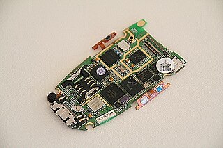
A printed circuit board (PCB) is a laminated sandwich structure of conductive and insulating layers. PCBs have two complementary functions. The first is to affix electronic components in designated locations on the outer layers by means of soldering. The second is to provide reliable electrical connections between the component's terminals in a controlled manner often referred to as PCB design. Each of the conductive layers is designed with an artwork pattern of conductors that provides electrical connections on that conductive layer. Another manufacturing process adds vias, plated-through holes that allow interconnections between layers.

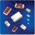
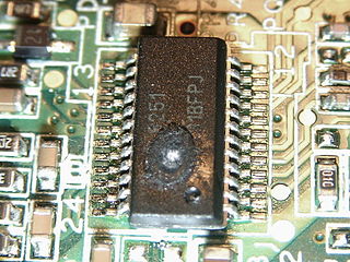
Surface-mount technology (SMT) is a method in which the electrical components are mounted directly onto the surface of a printed circuit board (PCB). An electrical component mounted in this manner is referred to as a surface-mount device (SMD). In industry, this approach has largely replaced the through-hole technology construction method of fitting components, in large part because SMT allows for increased manufacturing automation which reduces cost and improves quality. It also allows for more components to fit on a given area of substrate. Both technologies can be used on the same board, with the through-hole technology often used for components not suitable for surface mounting such as large transformers and heat-sinked power semiconductors.
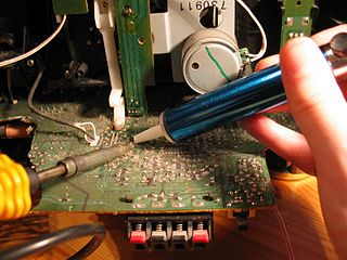
In electronics, desoldering is the removal of solder and components from a circuit board for troubleshooting, repair, replacement, and salvage.

Through-hole technology, refers to the mounting scheme used for electronic components that involves the use of leads on the components that are inserted into holes drilled in printed circuit boards (PCB) and soldered to pads on the opposite side either by manual assembly or by the use of automated insertion mount machines.
Rework is the term for the refinishing operation or repair of an electronic printed circuit board (PCB) assembly, usually involving desoldering and re-soldering of surface-mounted electronic components (SMD). Mass processing techniques are not applicable to single device repair or replacement, and specialized manual techniques by expert personnel using appropriate equipment are required to replace defective components; area array packages such as ball grid array (BGA) devices particularly require expertise and appropriate tools. A hot air gun or hot air station is used to heat devices and melt solder, and specialised tools are used to pick up and position often tiny components.

SMT component placement systems, commonly called pick-and-place machines or P&Ps, are robotic machines which are used to place surface-mount devices (SMDs) onto a printed circuit board (PCB). They are used for high speed, high precision placing of a broad range of electronic components, like capacitors, resistors, integrated circuits onto the PCBs which are in turn used in computers, consumer electronics as well as industrial, medical, automotive, military and telecommunications equipment. Similar equipment exists for through-hole components. This type of equipment is sometimes also used to package microchips using the flip chip method.
A hybrid integrated circuit (HIC), hybrid microcircuit, hybrid circuit or simply hybrid is a miniaturized electronic circuit constructed of individual devices, such as semiconductor devices and passive components, bonded to a substrate or printed circuit board (PCB). A PCB having components on a Printed Wiring Board (PWB) is not considered a true hybrid circuit according to the definition of MIL-PRF-38534.

The TO-220 is a style of electronic package used for high-powered, through-hole components with 0.1 inches (2.54 mm) pin spacing. The "TO" designation stands for "transistor outline". TO-220 packages have three leads. Similar packages with two, four, five or seven leads are also manufactured. A notable characteristic is a metal tab with a hole, used in mounting the case to a heatsink, allowing the component to dissipate more heat than one constructed in a TO-92 case. Common TO-220-packaged components include discrete semiconductors such as transistors and silicon-controlled rectifiers, as well as integrated circuits.

The thermal copper pillar bump, also known as the "thermal bump", is a thermoelectric device made from thin-film thermoelectric material embedded in flip chip interconnects for use in electronics and optoelectronic packaging, including: flip chip packaging of CPU and GPU integrated circuits (chips), laser diodes, and semiconductor optical amplifiers (SOA). Unlike conventional solder bumps that provide an electrical path and a mechanical connection to the package, thermal bumps act as solid-state heat pumps and add thermal management functionality locally on the surface of a chip or to another electrical component. The diameter of a thermal bump is 238 μm and 60 μm high.

Vishay Intertechnology, Inc. is an American manufacturer of discrete semiconductors and passive electronic components founded by Polish-born businessman Felix Zandman. Vishay has manufacturing plants in Israel, Asia, Europe, and the Americas where it produces rectifiers, diodes, MOSFETs, optoelectronics, selected integrated circuits, resistors, capacitors, and inductors. Vishay Intertechnology revenues for 2018 were $3.035 billion. As of December 31, 2018, Vishay Intertechnology had approximately 24,100 full-time employees.

A soldering station is a multipurpose power soldering device designed for electronic components soldering. This type of equipment is mostly used in electronics and electrical engineering. Soldering station consists of one or more soldering tools connected to the main unit, which includes the controls, means of indication, and may be equipped with an electric transformer. Soldering stations may include some accessories – holders and stands, soldering tip cleaners, etc.
Integrated Passive Devices (IPDs) or Integrated Passive Components (IPCs) or Embedded Passive Components are electronic components where resistors (R), capacitors (C), inductors (L)/coils/chokes, microstriplines, impedance matching elements, baluns or any combinations of them are integrated in the same package or on the same substrate. Sometimes integrated passives can also be called as embedded passives, and still the difference between integrated and embedded passives is technically unclear. In both cases passives are realized in between dielectric layers or on the same substrate.

Semikron is a German-based independent manufacturer of power semiconductor components. The company was founded in 1951 by Dr. Friedrich Josef Martin in Nuremberg. In 2019, the company has a staff of more than 3,000 people in 24 subsidiaries (world-wide) with production sites in Germany, Brazil, China, France, India, Italy, Slovakia and the USA.

Thick-film technology is used to produce electronic devices/modules such as surface mount devices modules, hybrid integrated circuits, heating elements, integrated passive devices and sensors. Main manufacturing technique is screen printing (stenciling), which in addition to use in manufacturing electronic devices can also be used for various graphic reproduction targets. It became one of the key manufacturing/miniaturisation techniques of electronic devices/modules during 1950s. Typical film thickness – manufactured with thick film manufacturing processes for electronic devices – is 0.0001 to 0.1 mm.
A semiconductor package is a metal, plastic, glass, or ceramic casing containing one or more discrete semiconductor devices or integrated circuits. Individual components are fabricated on semiconductor wafers before being diced into die, tested, and packaged. The package provides a means for connecting it to the external environment, such as printed circuit board, via leads such as lands, balls, or pins; and protection against threats such as mechanical impact, chemical contamination, and light exposure. Additionally, it helps dissipate heat produced by the device, with or without the aid of a heat spreader. There are thousands of package types in use. Some are defined by international, national, or industry standards, while others are particular to an individual manufacturer.
A QUADRAC is a special type of thyristor which combines a DIAC and a TRIAC in a single package. The DIAC is the triggering device for the TRIAC. Thyristors are four-layer (PNPN) semiconductor devices that act as switches, rectifiers or voltage regulators in a variety of applications. When triggered, thyristors turn on and become low-resistance current paths. They remain so even after the trigger is removed, and until the current is reduced to a certain level. Diacs are bi-directional diodes that switch AC voltages and trigger triacs or silicon-controlled rectifiers (SCRs). Except for a small leakage current, diacs do not conduct until the breakover voltage is reached. Triacs are three-terminal, silicon devices that function as two SCRs configured in an inverse, parallel arrangement. They provide load current during both halves of the AC supply voltage. By combining the functions of diacs and triacs, QUADRACs eliminate the need to buy and assemble discrete parts.
Electronic components have a wide range of failure modes. These can be classified in various ways, such as by time or cause. Failures can be caused by excess temperature, excess current or voltage, ionizing radiation, mechanical shock, stress or impact, and many other causes. In semiconductor devices, problems in the device package may cause failures due to contamination, mechanical stress of the device, or open or short circuits.
Component placement is an electronics manufacturing process that places electrical components precisely on printed circuit boards (PCBs) to create electrical interconnections between functional components and the interconnecting circuitry in the PCBs (leads-pads). The component leads must be accurately immersed in the solder paste previously deposited on the PCB pads. The next step after component placement is soldering.

