Ball grid array

Last updated
A grid array of solder balls on a printed circuit board after removal of an integrated circuit chip. Solder ball grid.jpg
A grid array of solder balls on a printed circuit board after removal of an integrated circuit chip.
Cross-cut section of BGA mounted circuit Bga und via IMGP4531 wp.jpg
Cross-cut section of BGA mounted circuit

A ball grid array (BGA) is a type of surface-mount packaging (a chip carrier) used for integrated circuits. BGA packages are used to permanently mount devices such as microprocessors. A BGA can provide more interconnection pins than can be put on a dual in-line or flat package. The whole bottom surface of the device can be used, instead of just the perimeter. The traces connecting the package's leads to the wires or balls which connect the die to package are also on average shorter than with a perimeter-only type, leading to better performance at high speeds.[ citation needed ]

Contents

BGAs were introduced in the 1990s and became popular by 2001. [1]

Soldering of BGA devices requires precise control and is usually done by automated processes such as in computer-controlled automatic reflow ovens.

Description

BGA ICs assembled on a Memory module BGA RAM.jpg
BGA ICs assembled on a Memory module

The BGA is descended from the pin grid array (PGA), which is a package with one face covered (or partly covered) with pins in a grid pattern which, in operation, conduct electrical signals between the integrated circuit and the printed circuit board (PCB) on which it is placed. In a BGA the pins are replaced by pads on the bottom of the package, each initially with a tiny solder ball stuck to it. These solder spheres can be placed manually or by automated equipment, and are held in place with a tacky flux. [2] The device is placed on a PCB with copper pads in a pattern that matches the solder balls. The assembly is then heated, either in a reflow oven or by an infrared heater, melting the balls. Surface tension causes the molten solder to hold the package in alignment with the circuit board, at the correct separation distance, while the solder cools and solidifies, forming soldered connections between the device and the PCB.

In more advanced technologies, solder balls may be used on both the PCB and the package. Also, in stacked multi-chip modules, (package on package) solder balls are used to connect two packages.

Advantages

High density

The BGA is a solution to the problem of producing a miniature package for an integrated circuit with many hundreds of pins. Pin grid arrays and dual-in-line surface mount (SOIC) packages were being produced with more and more pins, and with decreasing spacing between the pins, but this was causing difficulties for the soldering process. As package pins got closer together, the danger of accidentally bridging adjacent pins with solder grew.

Heat conduction

A further advantage of BGA packages over packages with discrete leads (i.e. packages with legs) is the lower thermal resistance between the package and the PCB. This allows heat generated by the integrated circuit inside the package to flow more easily to the PCB, preventing the chip from overheating.

Low-inductance leads

The shorter an electrical conductor, the lower its unwanted inductance, a property which causes unwanted distortion of signals in high-speed electronic circuits. BGAs, with their very short distance between the package and the PCB, have low lead inductances, giving them superior electrical performance to pinned devices.

Disadvantages

X-ray of BGA BGA joint xray.jpg
X-ray of BGA

Lack of compliance

A disadvantage of BGAs is that the solder balls cannot flex in the way that longer leads can, so they are not mechanically compliant. As with all surface mount devices, bending due to a difference in coefficient of thermal expansion between PCB substrate and BGA (thermal stress) or flexing and vibration (mechanical stress) can cause the solder joints to fracture.

Thermal expansion issues can be overcome by matching the mechanical and thermal characteristics of the PCB to those of the package. Typically, plastic BGA devices more closely match PCB thermal characteristics than ceramic devices.

The predominant use of RoHS compliant lead-free solder alloy assemblies has presented some further challenges to BGAs including "head in pillow" [3] soldering phenomenon, "pad cratering" problems as well as their decreased reliability versus lead-based solder BGAs in extreme operating conditions such as high temperature, high thermal shock and high gravitational force environments, in part due to lower ductility of RoHS-compliant solders. [4]

Mechanical stress issues can be overcome by bonding the devices to the board through a process called "underfilling", [5] which injects an epoxy mixture under the device after it is soldered to the PCB, effectively gluing the BGA device to the PCB. There are several types of underfill materials in use with differing properties relative to workability and thermal transfer. An additional advantage of underfill is that it limits tin whisker growth.

Another solution to non-compliant connections is to put a "compliant layer" in the package that allows the balls to physically move in relation to the package. This technique has become standard for packaging DRAMs in BGA packages.

Other techniques for increasing the board-level reliability of packages include use of low-expansion PCBs for ceramic BGA (CBGA) packages, interposers between the package and PCB, and re-packaging a device. [5]

Difficulty of inspection

Once the package is soldered into place, it is difficult to find soldering faults. X-ray machines, industrial CT scanning machines, [6] special microscopes, and endoscopes to look underneath the soldered package have been developed to overcome this problem. If a BGA is found to be badly soldered, it can be removed in a rework station , which is a jig fitted with infrared lamp (or hot air), a thermocouple and a vacuum device for lifting the package. The BGA can be replaced with a new one, or it can be refurbished (or reballed) and re-installed on the circuit board. Pre-configured solder balls matching the array pattern can be used to reball BGAs when only one or a few need to be reworked. For higher volume and repeated lab work, a stencil-configured vacuum-head pick-up and placement of loose spheres can be used.

Due to the cost of visual X-ray BGA inspection, electrical testing is very often used instead. Very common is boundary scan testing using an IEEE 1149.1 JTAG port.

A cheaper and easier inspection method, albeit destructive, is becoming increasingly popular because it does not require special equipment. Commonly referred to as dye and pry, the process includes immersing the entire PCB or just the BGA attached module into a dye, and after drying, the module is pried off and the broken joins are inspected. If a solder location contains the dye, then it indicates that the connection was imperfect. [7]

Difficulties during circuit development

During development it is not practical to solder BGAs into place, and sockets are used instead, but tend to be unreliable. There are two common types of socket: the more reliable type has spring pins that push up under the balls, although it does not allow using BGAs with the balls removed as the spring pins may be too short.

The less reliable type is a ZIF socket, with spring pinchers that grab the balls. This does not work well, especially if the balls are small.[ citation needed ]

Cost of equipment

Expensive equipment is required to reliably solder BGA packages; hand-soldering BGA packages is very difficult and unreliable, usable only for the smallest packages in the smallest quantities. [8] However, as more ICs have become available only in leadless (e.g. quad-flat no-leads package) or BGA packages, various DIY reflow methods have been developed using inexpensive heat sources such as heat guns, and domestic toaster ovens and electric skillets. [9]

Variants

Intel Mobile Celeron in a flip-chip BGA2 package (FCBGA-479); the die appears dark blue. Here the die has been mounted to a printed circuit board substrate below it (dark yellow, also called an interposer) using flip chip and underfill. Celeron mobile.jpg
Intel Mobile Celeron in a flip-chip BGA2 package (FCBGA-479); the die appears dark blue. Here the die has been mounted to a printed circuit board substrate below it (dark yellow, also called an interposer) using flip chip and underfill.
Inside a wire bond BGA package; this package has an Nvidia GeForce 256 GPU NVIDIA@220nm@Fixed-pipline@NV10@GeForce 256@T5A3202220008 S1 Taiwan A DSC01376 (29588383793).jpg
Inside a wire bond BGA package; this package has an Nvidia GeForce 256 GPU

Effectively also the flip chip methods for mounting chip dies to a carrier is sort of a BGA design derivate with the functional equivalent of the balls there being called bumps or micro bumps. This is realized at an already microscopic size level.

To make it easier to use ball grid array devices, most BGA packages only have balls in the outer rings of the package, leaving the innermost square empty.

Intel used a package designated BGA1 for their Pentium II and early Celeron mobile processors. BGA2 is Intel's package for their Pentium III and some later Celeron mobile processors. BGA2 is also known as FCBGA-479. It replaced its predecessor, BGA1.

For example, the "micro-FCBGA" (flip chip ball grid array) is Intel's current[ when? ] BGA mounting method for mobile processors that use a flip chip binding technology. It was introduced with the Coppermine Mobile Celeron.[ citation needed ] Micro-FCBGA has 479 balls that are 0.78 mm in diameter. The processor is affixed to the motherboard by soldering the balls to the motherboard. This is thinner than a pin grid array socket arrangement, but is not removable.

The 479 balls of the Micro-FCBGA package (a package almost identical to the 478-pin socketable micro-FCPGA package) are arranged as the 6 outer rings of a 1.27 mm pitch (20 balls per inch pitch) 26x26 square grid, with the inner 14x14 region empty. [12] [13]

Procurement

Primary end-users of BGAs are original equipment manufacturers (OEMs). There is also a market among electronic hobbyists do it yourself (DIY) such as the increasingly popular maker movement. [14] While OEMs generally source their components from the manufacturer, or the manufacturer's distributor, the hobbyist will typically obtain BGAs on the aftermarket through electronic component brokers or distributors.

See also

Related Research Articles

<span class="mw-page-title-main">Dual in-line package</span> Type of electronic component package

In microelectronics, a dual in-line package is an electronic component package with a rectangular housing and two parallel rows of electrical connecting pins. The package may be through-hole mounted to a printed circuit board (PCB) or inserted in a socket. The dual-inline format was invented by Don Forbes, Rex Rice and Bryant Rogers at Fairchild R&D in 1964, when the restricted number of leads available on circular transistor-style packages became a limitation in the use of integrated circuits. Increasingly complex circuits required more signal and power supply leads ; eventually microprocessors and similar complex devices required more leads than could be put on a DIP package, leading to development of higher-density chip carriers. Furthermore, square and rectangular packages made it easier to route printed-circuit traces beneath the packages.

<span class="mw-page-title-main">Zero insertion force</span> Electrical socket

Zero insertion force (ZIF) is a type of IC socket or electrical connector that requires very little force for insertion. With a ZIF socket, before the IC is inserted, a lever or slider on the side of the socket is moved, pushing all the sprung contacts apart so that the IC can be inserted with very little force - generally the weight of the IC itself is sufficient and no external downward force is required. The lever is then moved back, allowing the contacts to close and grip the pins of the IC. ZIF sockets are much more expensive than standard IC sockets and also tend to take up a larger board area due to the space taken up by the lever mechanism. Typically, they are only used when there is a good reason to do so.

<span class="mw-page-title-main">Surface-mount technology</span> Method for producing electronic circuits

Surface-mount technology (SMT), originally called planar mounting, is a method in which the electrical components are mounted directly onto the surface of a printed circuit board (PCB). An electrical component mounted in this manner is referred to as a surface-mount device (SMD). In industry, this approach has largely replaced the through-hole technology construction method of fitting components, in large part because SMT allows for increased manufacturing automation which reduces cost and improves quality. It also allows for more components to fit on a given area of substrate. Both technologies can be used on the same board, with the through-hole technology often used for components not suitable for surface mounting such as large transformers and heat-sinked power semiconductors.

<span class="mw-page-title-main">Pin grid array</span> Type of integrated circuit packaging with the pins mounted on the underside of the package

A pin grid array (PGA) is a type of integrated circuit packaging. In a PGA, the package is square or rectangular, and the pins are arranged in a regular array on the underside of the package. The pins are commonly spaced 2.54 mm (0.1") apart, and may or may not cover the entire underside of the package.

<span class="mw-page-title-main">Flip chip</span> Technique that flips a microchip upside down to connect it

Flip chip, also known as controlled collapse chip connection or its abbreviation, C4, is a method for interconnecting dies such as semiconductor devices, IC chips, integrated passive devices and microelectromechanical systems (MEMS), to external circuitry with solder bumps that have been deposited onto the chip pads. The technique was developed by General Electric's Light Military Electronics Department, Utica, New York. The solder bumps are deposited on the chip pads on the top side of the wafer during the final wafer processing step. In order to mount the chip to external circuitry, it is flipped over so that its top side faces down, and aligned so that its pads align with matching pads on the external circuit, and then the solder is reflowed to complete the interconnect. This is in contrast to wire bonding, in which the chip is mounted upright and fine wires are welded onto the chip pads and lead frame contacts to interconnect the chip pads to external circuitry.

<span class="mw-page-title-main">Integrated circuit packaging</span> Final stage of semiconductor device fabrication

Integrated circuit packaging is the final stage of semiconductor device fabrication, in which the die is encapsulated in a supporting case that prevents physical damage and corrosion. The case, known as a "package", supports the electrical contacts which connect the device to a circuit board.

<span class="mw-page-title-main">CPU socket</span> Circuit board-microprocessor connection

In computer hardware, a CPU socket or CPU slot contains one or more mechanical components providing mechanical and electrical connections between a microprocessor and a printed circuit board (PCB). This allows for placing and replacing the central processing unit (CPU) without soldering.

<span class="mw-page-title-main">Land grid array</span> Type of surface-mount packaging for integrated circuits

The land grid array (LGA) is a type of surface-mount packaging for integrated circuits (ICs) that is notable for having the pins on the socket — as opposed to pins on the integrated circuit, known as a pin grid array (PGA). An LGA can be electrically connected to a printed circuit board (PCB) either by the use of a socket or by soldering directly to the board.

<span class="mw-page-title-main">Quad flat package</span> Surface mount integrated circuit package with "gull wing" pins extending from all sides

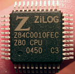
A quad flat package (QFP) is a surface-mounted integrated circuit package with "gull wing" leads extending from each of the four sides. Socketing such packages is rare and through-hole mounting is not possible. Versions ranging from 32 to 304 pins with a pitch ranging from 0.4 to 1.0 mm are common. Other special variants include low-profile QFP (LQFP) and thin QFP (TQFP).

<span class="mw-page-title-main">Rework (electronics)</span> Refinishing operation of an electronic printed circuit board assembly

Rework is the term for the refinishing operation or repair of an electronic printed circuit board (PCB) assembly, usually involving desoldering and re-soldering of surface-mounted electronic components (SMD). Mass processing techniques are not applicable to single device repair or replacement, and specialized manual techniques by expert personnel using appropriate equipment are required to replace defective components; area array packages such as ball grid array (BGA) devices particularly require expertise and appropriate tools. A hot air gun or hot air station is used to heat devices and melt solder, and specialised tools are used to pick up and position often tiny components.

<span class="mw-page-title-main">Socket 479</span>

Socket 479 (mPGA479M) is the CPU socket for the Intel Pentium M and Celeron M mobile processors normally used in laptops, but has also been used with Tualatin-M Pentium III processors. The official naming by Intel is µFCPGA and µPGA479M.

<span class="mw-page-title-main">Flat no-leads package</span> Integrated circuit package with contacts on all 4 sides, on the underside of the package

Flat no-leads packages such as quad-flat no-leads (QFN) and dual-flat no-leads (DFN) physically and electrically connect integrated circuits to printed circuit boards. Flat no-leads, also known as micro leadframe (MLF) and SON, is a surface-mount technology, one of several package technologies that connect ICs to the surfaces of PCBs without through-holes. Flat no-lead is a near chip scale plastic encapsulated package made with a planar copper lead frame substrate. Perimeter lands on the package bottom provide electrical connections to the PCB. Flat no-lead packages usually, but not always, include an exposed thermally conductive pad to improve heat transfer out of the IC. Heat transfer can be further facilitated by metal vias in the thermal pad. The QFN package is similar to the quad-flat package (QFP), and a ball grid array (BGA).

Package on a package (PoP) is an integrated circuit packaging method to vertically combine discrete logic and memory ball grid array (BGA) packages. Two or more packages are installed atop each other, i.e. stacked, with a standard interface to route signals between them. This allows higher component density in devices, such as mobile phones, personal digital assistants (PDA), and digital cameras, at the cost of slightly higher height requirements. Stacks with more than 2 packages are uncommon, due to heat dissipation considerations.

<span class="mw-page-title-main">Socket 495</span>

Socket 495, also known as µPGA2, is a CPU socket used for the Intel Pentium III and Celeron mobile processors. This socket was also used in Microsoft's Xbox console for the Xbox CPU, albeit in a BGA format. It replaces Socket 615 (µPGA1), which was used in Pentium II and early Celeron mobile processors.

Pad cratering is a mechanically induced fracture in the resin between copper foil and outermost layer of fiberglass of a printed circuit board (PCB). It may be within the resin or at the resin to fiberglass interface.

<span class="mw-page-title-main">Chip carrier</span> Surface mount technology package for integrated circuits

In electronics, a chip carrier is one of several kinds of surface-mount technology packages for integrated circuits. Connections are made on all four edges of a square package; compared to the internal cavity for mounting the integrated circuit, the package overall size is large.

<span class="mw-page-title-main">Solder ball</span>

In integrated circuit packaging, a solder ball, also a solder bump is a ball of solder that provides the contact between the chip package and the printed circuit board, as well as between stacked packages in multichip modules; in the latter case, they may be referred to as microbumps, since they are usually significantly smaller than the former. The solder balls can be placed manually or by automated equipment, and are held in place with a tacky flux.

Digital image correlation analyses have applications in material property characterization, displacement measurement, and strain mapping. As such, DIC is becoming an increasingly popular tool when evaluating the thermo-mechanical behavior of electronic components and systems.

<span class="mw-page-title-main">Chip on board</span> Method of circuit board manufacture

Chip on board (COB) is a method of circuit board manufacturing in which the integrated circuits (e.g. microprocessors) are attached (wired, bonded directly) to a printed circuit board, and covered by a blob of epoxy. By eliminating the packaging of individual semiconductor devices, the completed product can be more compact, lighter, and less costly. In some cases, COB construction improves the operation of radio frequency systems by reducing the inductance and capacitance of integrated circuit leads.

References

  1. "Ball Grid Array (BGA) - Engineering Technical - PCBway".
  2. "Soldering 101 - A Basic Overview". Archived from the original on 2012-03-03. Retrieved 2010-12-29.
  3. Alpha (2010-03-15) [September 2009]. "Reducing Head in Pillow Defects - Head in pillow defects: causes and potential solutions". 3. Archived from the original on 2013-12-03. Retrieved 2018-06-18.
  4. "TEERM - TEERM Active Project - NASA-DOD Lead-Free Electronics (Project 2)". Teerm.nasa.gov. Archived from the original on 2014-10-08. Retrieved 2014-03-21.
  5. 1 2 Solid State Technology: BGA underfills - Increasing board-level solder joint reliability, 12/01/2001
  6. "CT Services - Overview." Jesse Garant & Associates. August 17, 2010. "Industrial Computed Tomography Scanning Services – JG&A". Archived from the original on 2010-09-23. Retrieved 2010-11-24.
  7. "Dye and Pry of BGA Solder Joints" (PDF). cascade-eng.com. 2013-11-22. Archived from the original (PDF) on 2011-10-16. Retrieved 2014-03-22.
  8. Das, Santosh (2019-08-22). "BGA Soldering & Repairing / How to Solder Ball Grid Array". Electronics and You. Retrieved 2021-09-07.
  9. Sparkfun tutorials: Reflow skillet, July 2006
  10. Design Requirements - Fine Pitch Ball Grid Array Package (FBGA) DR-4.27D, jedec.org, MAR 2017
  11. Ryan J. Leng. "The Secrets of PC Memory: Part 2". 2007.
  12. Intel. "Mobile Intel Celeron Processor (0.13 μ) in Micro-FCBGA and Micro-FCPGA Packages". Datasheet Archived 2014-03-18 at the Wayback Machine . 2002.
  13. "FCBGA-479 (Micro-FCBGA)". Archived from the original on 2021-02-28. Retrieved 2011-12-20.
  14. "More than just digital quilting: The "maker" movement could change how science is taught and boost innovation. It may even herald a new industrial revolution". The Economist. Dec 3, 2011.