
An integrated circuit (IC), also known as a microchip, computer chip, or simply chip, is a small electronic device made up of multiple interconnected electronic components such as transistors, resistors, and capacitors. These components are etched onto a small piece of semiconductor material, usually silicon. Integrated circuits are used in a wide range of electronic devices, including computers, smartphones, and televisions, to perform various functions such as processing and storing information. They have greatly impacted the field of electronics by enabling device miniaturization and enhanced functionality.

A motherboard is the main printed circuit board (PCB) in general-purpose computers and other expandable systems. It holds and allows communication between many of the crucial electronic components of a system, such as the central processing unit (CPU) and memory, and provides connectors for other peripherals. Unlike a backplane, a motherboard usually contains significant sub-systems, such as the central processor, the chipset's input/output and memory controllers, interface connectors, and other components integrated for general use.

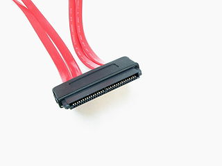
SATA is a computer bus interface that connects host bus adapters to mass storage devices such as hard disk drives, optical drives, and solid-state drives. Serial ATA succeeded the earlier Parallel ATA (PATA) standard to become the predominant interface for storage devices.
JTAG is an industry standard for verifying designs of and testing printed circuit boards after manufacture.

The land grid array (LGA) is a type of surface-mount packaging for integrated circuits (ICs) that is notable for having the pins on the socket — as opposed to pins on the integrated circuit, known as a pin grid array (PGA). An LGA can be electrically connected to a printed circuit board (PCB) either by the use of a socket or by soldering directly to the board.

Xilinx, Inc. was an American technology and semiconductor company that primarily supplied programmable logic devices. The company is known for inventing the first commercially viable field-programmable gate array (FPGA). It also created the first fabless manufacturing model.
In computing, Serial Attached SCSI (SAS) is a point-to-point serial protocol that moves data to and from computer-storage devices such as hard disk drives and tape drives. SAS replaces the older Parallel SCSI bus technology that first appeared in the mid-1980s. SAS, like its predecessor, uses the standard SCSI command set. SAS offers optional compatibility with Serial ATA (SATA), versions 2 and later. This allows the connection of SATA drives to most SAS backplanes or controllers. The reverse, connecting SAS drives to SATA backplanes, is not possible.

A multi-chip module (MCM) is generically an electronic assembly where multiple integrated circuits, semiconductor dies and/or other discrete components are integrated, usually onto a unifying substrate, so that in use it can be treated as if it were a larger IC. Other terms for MCM packaging include "heterogeneous integration" or "hybrid integrated circuit". The advantage of using MCM packaging is it allows a manufacturer to use multiple components for modularity and/or to improve yields over a conventional monolithic IC approach.

A system in a package (SiP) or system-in-package is a number of integrated circuits (ICs) enclosed in one chip carrier package or encompassing an IC package substrate that may include passive components and perform the functions of an entire system. The ICs may be stacked using package on package, placed side by side, and/or embedded in the substrate. The SiP performs all or most of the functions of an electronic system, and is typically used when designing components for mobile phones, digital music players, etc. Dies containing integrated circuits may be stacked vertically on the package substrate. They are internally connected by fine wires that are bonded to the package substrate. Alternatively, with a flip chip technology, solder bumps are used to join stacked chips together and to the package substrate, or even both techniques can be used in a single package. SiPs are like systems on a chip (SoCs) but less tightly integrated and not on a single semiconductor die.

In computing, a memory module or RAM stick is a printed circuit board on which memory integrated circuits are mounted.

In electronic engineering, a through-silicon via (TSV) or through-chip via is a vertical electrical connection (via) that passes completely through a silicon wafer or die. TSVs are high-performance interconnect techniques used as an alternative to wire-bond and flip chips to create 3D packages and 3D integrated circuits. Compared to alternatives such as package-on-package, the interconnect and device density is substantially higher, and the length of the connections becomes shorter.
A three-dimensional integrated circuit is a MOS integrated circuit (IC) manufactured by stacking as many as 16 or more ICs and interconnecting them vertically using, for instance, through-silicon vias (TSVs) or Cu-Cu connections, so that they behave as a single device to achieve performance improvements at reduced power and smaller footprint than conventional two dimensional processes. The 3D IC is one of several 3D integration schemes that exploit the z-direction to achieve electrical performance benefits in microelectronics and nanoelectronics.

Integrated passive devices (IPDs), also known as integrated passive components (IPCs) or embedded passive components (EPC), are electronic components where resistors (R), capacitors (C), inductors (L)/coils/chokes, microstriplines, impedance matching elements, baluns or any combinations of them are integrated in the same package or on the same substrate. Sometimes integrated passives can also be called as embedded passives, and still the difference between integrated and embedded passives is technically unclear. In both cases passives are realized in between dielectric layers or on the same substrate.

Wafer-level packaging (WLP) is a process in integrated circuit manufacturing where packaging components are attached to an integrated circuit (IC) before the wafer – on which the IC is fabricated – is diced. In WLP, the top and bottom layers of the packaging and the solder bumps are attached to the integrated circuits while they are still in the wafer. This process differs from a conventional process, in which the wafer is sliced into individual circuits (dice) before the packaging components are attached.
Virtex is the flagship family of FPGA products currently developed by AMD, originally Xilinx before being acquired by the former. Other current product lines include Kintex (mid-range) and Artix (low-cost), each including configurations and models optimized for different applications. In addition, AMD offers the Spartan low-cost series, which continues to be updated and is nearing production utilizing the same underlying architecture and process node as the larger 7-series devices.
Hybrid Memory Cube (HMC) is a high-performance computer random-access memory (RAM) interface for through-silicon via (TSV)-based stacked DRAM memory. HMC competes with the incompatible rival interface High Bandwidth Memory (HBM).
High Bandwidth Memory (HBM) is a computer memory interface for 3D-stacked synchronous dynamic random-access memory (SDRAM) initially from Samsung, AMD and SK Hynix. It is used in conjunction with high-performance graphics accelerators, network devices, high-performance datacenter AI ASICs, as on-package cache in CPUs and on-package RAM in upcoming CPUs, and FPGAs and in some supercomputers. The first HBM memory chip was produced by SK Hynix in 2013, and the first devices to use HBM were the AMD Fiji GPUs in 2015.
A 2.5D integrated circuit is an advanced packaging technique that combines multiple integrated circuit dies in a single package without stacking them into a three-dimensional integrated circuit (3D-IC) with through-silicon vias (TSVs). The term "2.5D" originated when 3D-ICs with TSVs were quite new and still very difficult. Chip designers realized that many of the advantages of 3D integration could be approximated by placing bare dies side by side on an interposer instead of stacking them vertically. If the pitch is very fine and the interconnect very short, the assembly can be packaged as a single component with better size, weight, and power characteristics than a comparable 2D circuit board assembly. This half-way 3D integration was facetiously named "2.5D" and the name stuck. Since then, 2.5D has proven to be far more than just "half-way to 3D." Some benefits:
Glossary of microelectronics manufacturing terms
Advanced packaging is the aggregation and interconnection of components before traditional integrated circuit packaging where a single die is packaged. Advanced packaging allows multiple devices, including electrical, mechanical, or semiconductor devices, to be merged and packaged as a single electronic device. Advanced packaging uses processes and techniques that are typically performed at semiconductor fabrication facilities, unlike traditional integrated circuit packaging, which does not. Advanced packaging thus sits between fabrication and traditional packaging -- or, in other terminology, between BEoL and post-fab. Advanced packaging includes multi-chip modules, 3D ICs, 2.5D ICs, heterogeneous integration, fan-out wafer-level packaging, system-in-package, quilt packaging, combining logic (processors) and memory in a single package, die stacking, several chiplets or dies in a package, combinations of these techniques, and others. 2.5D and 3D ICs are also called 2.5D or 3D packages.

