
A printed circuit board (PCB), also called printed wiring board (PWB), is a medium used to connect or "wire" components to one another in a circuit. It takes the form of a laminated sandwich structure of conductive and insulating layers: each of the conductive layers is designed with an artwork pattern of traces, planes and other features etched from one or more sheet layers of copper laminated onto and/or between sheet layers of a non-conductive substrate. Electrical components may be fixed to conductive pads on the outer layers in the shape designed to accept the component's terminals, generally by means of soldering, to both electrically connect and mechanically fasten them to it. Another manufacturing process adds vias, plated-through holes that allow interconnections between layers.

A ball grid array (BGA) is a type of surface-mount packaging used for integrated circuits. BGA packages are used to permanently mount devices such as microprocessors. A BGA can provide more interconnection pins than can be put on a dual in-line or flat package. The whole bottom surface of the device can be used, instead of just the perimeter. The traces connecting the package's leads to the wires or balls which connect the die to package are also on average shorter than with a perimeter-only type, leading to better performance at high speeds.

Surface-mount technology (SMT), originally called planar mounting, is a method in which the electrical components are mounted directly onto the surface of a printed circuit board (PCB). An electrical component mounted in this manner is referred to as a surface-mount device (SMD). In industry, this approach has largely replaced the through-hole technology construction method of fitting components, in large part because SMT allows for increased manufacturing automation which reduces cost and improves quality. It also allows for more components to fit on a given area of substrate. Both technologies can be used on the same board, with the through-hole technology often used for components not suitable for surface mounting such as large transformers and heat-sinked power semiconductors.

Flip chip, also known as controlled collapse chip connection or its abbreviation, C4, is a method for interconnecting dies such as semiconductor devices, IC chips, integrated passive devices and microelectromechanical systems (MEMS), to external circuitry with solder bumps that have been deposited onto the chip pads. The technique was developed by General Electric's Light Military Electronics Department, Utica, New York. The solder bumps are deposited on the chip pads on the top side of the wafer during the final wafer processing step. In order to mount the chip to external circuitry, it is flipped over so that its top side faces down, and aligned so that its pads align with matching pads on the external circuit, and then the solder is reflowed to complete the interconnect. This is in contrast to wire bonding, in which the chip is mounted upright and fine wires are welded onto the chip pads and lead frame contacts to interconnect the chip pads to external circuitry.

A reflow oven is a machine used primarily for reflow soldering of surface mount electronic components to printed circuit boards (PCBs).
In electronics, desoldering is the removal of solder and components from a circuit board for troubleshooting, repair, replacement, and salvage.

Wave soldering is a bulk soldering process used for the manufacturing of printed circuit boards. The circuit board is passed over a pan of molten solder in which a pump produces an upwelling of solder that looks like a standing wave. As the circuit board makes contact with this wave, the components become soldered to the board. Wave soldering is used for both through-hole printed circuit assemblies, and surface mount. In the latter case, the components are glued onto the surface of a printed circuit board (PCB) by placement equipment, before being run through the molten solder wave. Wave soldering is mainly used in soldering of through hole components.

Reflow soldering is a process in which a solder paste is used to temporarily attach one or thousands of tiny electrical components to their contact pads, after which the entire assembly is subjected to controlled heat. The solder paste reflows in a molten state, creating permanent solder joints. Heating may be accomplished by passing the assembly through a reflow oven, under an infrared lamp, or by soldering individual joints with a hot air pencil.

Solder paste is used in the manufacture of printed circuit boards to connect surface mount components to pads on the board. It is also possible to solder through-hole pin in paste components by printing solder paste in and over the holes. The sticky paste temporarily holds components in place; the board is then heated, melting the paste and forming a mechanical bond as well as an electrical connection. The paste is applied to the board by jet printing, stencil printing or syringe; then the components are put in place by a pick-and-place machine or by hand.

Selective soldering is the process of selectively soldering components to printed circuit boards and molded modules that could be damaged by the heat of a reflow oven or wave soldering in a traditional surface-mount technology (SMT) or through-hole technology assembly processes. This usually follows an SMT oven reflow process; parts to be selectively soldered are usually surrounded by parts that have been previously soldered in a surface-mount reflow process, and the selective-solder process must be sufficiently precise to avoid damaging them.

Flat no-leads packages such as quad-flat no-leads (QFN) and dual-flat no-leads (DFN) physically and electrically connect integrated circuits to printed circuit boards. Flat no-leads, also known as micro leadframe (MLF) and SON, is a surface-mount technology, one of several package technologies that connect ICs to the surfaces of PCBs without through-holes. Flat no-lead is a near chip scale plastic encapsulated package made with a planar copper lead frame substrate. Perimeter lands on the package bottom provide electrical connections to the PCB. Flat no-lead packages usually, but not always, include an exposed thermally conductive pad to improve heat transfer out of the IC. Heat transfer can be further facilitated by metal vias in the thermal pad. The QFN package is similar to the quad-flat package (QFP), and a ball grid array (BGA).
Automated optical inspection (AOI) is an automated visual inspection of printed circuit board (PCB) manufacture where a camera autonomously scans the device under test for both catastrophic failure and quality defects. It is commonly used in the manufacturing process because it is a non-contact test method. It is implemented at many stages through the manufacturing process including bare board inspection, solder paste inspection (SPI), pre-reflow and post-re-flow as well as other stages.
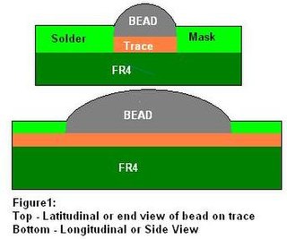
Bead probe technology (BPT) is technique used to provide electrical access to printed circuit board (PCB) circuitry for performing in-circuit testing (ICT). It makes use of small beads of solder placed onto the board's traces to allow measuring and controlling of the signals using a test probe. This permits test access to boards on which standard ICT test pads are not feasible due to space constraints.

A soldering station is a multipurpose power soldering device designed for electronic components soldering. This type of equipment is mostly used in electronics and electrical engineering. Soldering station consists of one or more soldering tools connected to the main unit, which includes the controls, means of indication, and may be equipped with an electric transformer. Soldering stations may include some accessories – holders and stands, soldering tip cleaners, etc.

A thermal profile is a complex set of time-temperature data typically associated with the measurement of thermal temperatures in an oven. The thermal profile is often measured along a variety of dimensions such as slope, soak, time above liquidus (TAL), and peak.

Soldering is a process of joining two metal surfaces together using a filler metal called solder. The soldering process involves heating the surfaces to be joined and melting the solder, which is then allowed to cool and solidify, creating a strong and durable joint.
Pad cratering is a mechanically induced fracture in the resin between copper foil and outermost layer of fiberglass of a printed circuit board (PCB). It may be within the resin or at the resin to fiberglass interface.
In the assembly of integrated circuit packages to printed circuit boards, a head-in-pillow defect, also called ball-and-socket, is a failure of the soldering process. For example, in the case of a ball grid array (BGA) package, the pre-deposited solder ball on the package and the solder paste applied to the circuit board may both melt, but the melted solder does not join. A cross-section through the failed joint shows a distinct boundary between the solder ball on the part and the solder paste on the circuit board, rather like a section through a head resting on a pillow.
Digital image correlation analyses have applications in material property characterization, displacement measurement, and strain mapping. As such, DIC is becoming an increasingly popular tool when evaluating the thermo-mechanical behavior of electronic components and systems.

Chip on board (COB) is a method of circuit board manufacturing in which the integrated circuits (e.g. microprocessors) are attached (wired, bonded directly) to a printed circuit board, and covered by a blob of epoxy. By eliminating the packaging of individual semiconductor devices, the completed product can be more compact, lighter, and less costly. In some cases, COB construction improves the operation of radio frequency systems by reducing the inductance and capacitance of integrated circuit leads.


