TO-5

Last updated
Transistor in a TO-5 package with 25 mm leads. SF122C HFO.jpg
Transistor in a TO-5 package with 25 mm leads.
Gear-shaped heat sinks for TO-5 packages. TO-5 Heatsinks.jpg
Gear-shaped heat sinks for TO-5 packages.

In electronics, TO-5 is a designation for a standardized metal semiconductor package used for transistors and some integrated circuits. The TO element stands for "transistor outline" and refers to a series of technical drawings produced by JEDEC. [1] The first commercial silicon transistors, the 2N696 and 2N697 from Fairchild Semiconductor, came in a TO-5 package. [2]

Contents

Construction and orientation

The tab is located 45° from pin 1, which is typically the emitter. The typical TO-5 package has a base diameter of 8.9 mm (0.35 in), a cap diameter of 8.1 mm (0.32 in), a cap height of 6.3 mm (0.25 in). [1] The pins are isolated from the package by individual glass-metal seals, or by a single resin potting. Sometimes one pin is connected directly to the metal case.

Variants

Several variants of the original TO-5 package have the same cap dimensions but differ in the number and length of the leads (wires). Somewhat incorrectly, TO-5 and TO-39 are often used in manufacturer's literature as synonyms for any package with the cap dimensions of TO-5, regardless of the number of leads, or even for any package with the diameter of TO-5, regardless of the cap height and the number of leads. [3] Compared to TO-5, for the other variants (except TO-33 and TO-42) the minimum length of the leads was shortened from 38.1 mm (1.50 in) to 12.7 mm (0.50 in) which is sufficient for through-hole technology and leads to a cost reduction, whereas the longer leads were needed for point-to-point construction. Lead lengths of 25.4 mm (1.00 in) and 19.05 mm (0.750 in) are quite common but were not standardized separately by JEDEC. There are variants with between 2 and 12 leads. The leads are arranged in a circle with a diameter of 5.08 mm (0.200 in) (except TO-96, TO-97, TO-100, TO-101). Before the introduction of dual in-line packages in 1965, integrated circuits were packaged mostly in metal can packages such as the TO-5 variants with more than 3 leads. [4]

TO-39 / TO-9 / TO-16 / TO-42

The TO-39, TO-9, and TO-16 packages have 3 leads and differ in the shortened leads mentioned above from TO-5. [5] Additionally, the TO-9 and TO-16 packages do not have a tab. [6] The TO-42 package is almost identical to the TO-5 package (including the long leads) but has four stand-offs at the bottom of the base that keep the base about 0.5 mm above the circuit board. [7] Possibly the TO-16 and TO-42 designations were not actually used. [2]

TO-12 / TO-33

Resistive opto-isolator VTL2C1 in a TO-33 package Perkin Elmer VTL2C1 cm.jpg
Resistive opto-isolator VTL2C1 in a TO-33 package

The TO-12 and TO-33 packages have 4 leads. [8] TO-33 has 38.1 mm (1.50 in) leads [9] like TO-5 while TO-12 has 12.7 mm (0.50 in) leads. For transistors, the fourth wire is typically connected to the metal case as a means of electromagnetic shielding for radio frequency applications.

TO-75

The TO-75 package has 6 leads (at most one of those may be omitted). [10] The minimum angle between two adjacent leads is 60°.

TO-76 / TO-77

Voltage regulator integrated circuit (Tesla MAA723) in a TO-76 package. Tesla MAA723.jpg
Voltage regulator integrated circuit (Tesla MAA723) in a TO-76 package.

The TO-76 and TO-77 packages have 8 leads (up to three of those may be omitted). [11] The minimum angle between two adjacent leads is 45°. The TO-77 package differs from the TO-76 package only in that the bottom of a TO-77 package can sit directly on a circuit board whereas the TO-76 package requires a distance of up to 1.02 mm (0.040 in) between circuit board and package. [12]

TO-78 / TO-79 / TO-80 / TO-99

Sample-and-hold integrated circuit (Tesla MAC198) in a reduced-height TO-99 package. Tesla MAC198.jpg
Sample-and-hold integrated circuit (Tesla MAC198) in a reduced-height TO-99 package.

The TO-78, [13] TO-79, [14] TO-80, [15] and TO-99 [16] packages have 8 leads (up to three of those may be omitted). The minimum angle between two adjacent leads is 45°. These packages differ from other variants in the height of the cap. Instead of 6.3 mm (0.25 in) the cap height is only 4.45 mm (0.175 in) for TO-78 / TO-99, 3.81 mm (0.150 in) for TO-79, and 2.41 mm (0.095 in) for TO-80. The TO-78 package differs from the TO-99 package only in that the bottom of a TO-78 package can sit directly on a circuit board whereas the TO-99 package requires a distance of up to 1.02 mm (0.040 in) between circuit board and package.

TO-74

The TO-74 package has 10 leads (at most one of those may be omitted). [17] The minimum angle between two adjacent leads is 36°.

TO-96 / TO-97 / TO-100

The TO-96, [18] TO-97, [19] and TO-100 [20] packages have 10 leads (at most one of those may be omitted). The minimum angle between two adjacent leads is 36°. For these packages the diameter of the circle of leads is increased from 5.08 mm (0.200 in) to 5.84 mm (0.230 in). This allows a slightly increased chip area in a cap of unchanged diameter. TO-96 has the standard cap height of 6.3 mm (0.25 in), while TO-100 and TO-97 have reduced cap heights of 4.45 mm (0.175 in) (like TO-78) and 3.81 mm (0.150 in) (like TO-79), respectively.

TO-73

The TO-73 package has 12 leads (at most one of those may be omitted). [21] The minimum angle between two adjacent leads is 30°.

TO-101

The TO-101 package has 12 leads (at most one of those may be omitted). [22] The minimum angle between two adjacent leads is 30°. For this package the diameter of the circle of leads is increased from 5.08 mm (0.200 in) to 5.84 mm (0.230 in). This allows a slightly increased chip area in a cap of unchanged diameter. TO-101 has a reduced cap height of 4.45 mm (0.175 in) (like TO-78).

TO-205

Voltage reference integrated circuit (National Semiconductor LH0070) in a TO-205-AF package NatSemi LH0070.jpg
Voltage reference integrated circuit (National Semiconductor LH0070) in a TO-205-AF package

TO-205 is intended to replace previous definitions of packages with leads arranged in a circle with a diameter of 5.08 mm (0.200 in). [23] [24] The different outlines are now defined as variants of TO-205: TO-5 is renamed to TO-205-AA, TO-12 to TO-205-AB, TO-33 to TO-205-AC, TO-39 to TO-205-AD. A new package with 3 leads and a cap height of 4.32 mm (0.170 in) (similar to TO-78 / TO-99) is added as TO-205-AF.

National Standards

Standards organizationStandardDesignation for
TO-5TO-12TO-33TO-39TO-77
JEDEC JEP95 [24] TO-205-AATO-205-ABTO-205-ACTO-205-AD
IEC IEC 60191 [lower-alpha 1] [25] C4/B4AC4/B6CC4/B6AC4/B4CC4/B7C
DIN DIN 41873 [26] [25] 5A35C45C35C8
EIAJ / JEITA ED-7500A [lower-alpha 1] [27] TC5/TB-5ATC5/TB-14CTC5/TB-14ATC5/TB-5CTC5/TB-15C
British Standards BS 3934 [lower-alpha 1] [28] [25] SO-3/SB3-3ASO-3/SB4-1BSO-3/SB3-3BSO-3/SB8-1B
Gosstandart GOST 18472—88 [29] KT-2-12 [lower-alpha 2] KT-2-7 [lower-alpha 3]
Rosstandart GOST R 57439 [30]
Kombinat Mikroelektronik Erfurt TGL 11811 [31] B3/15-3a
TGL 26713/07 [31] F1BC3
  1. 1 2 3 These standards have separate drawings for the package case and the base.
  2. Russian: КТ-2-12
  3. Russian: КТ-2-7

Related Research Articles

<span class="mw-page-title-main">Semiconductor device fabrication</span> Manufacturing process used to create integrated circuits

Semiconductor device fabrication is the process used to manufacture semiconductor devices, typically integrated circuits (ICs) such as computer processors, microcontrollers, and memory chips that are present in everyday electronic devices. It is a multiple-step photolithographic and physio-chemical process during which electronic circuits are gradually created on a wafer, typically made of pure single-crystal semiconducting material. Silicon is almost always used, but various compound semiconductors are used for specialized applications.

<span class="mw-page-title-main">Dual in-line package</span> Type of electronic component package

In microelectronics, a dual in-line package is an electronic component package with a rectangular housing and two parallel rows of electrical connecting pins. The package may be through-hole mounted to a printed circuit board (PCB) or inserted in a socket. The dual-inline format was invented by Don Forbes, Rex Rice and Bryant Rogers at Fairchild R&D in 1964, when the restricted number of leads available on circular transistor-style packages became a limitation in the use of integrated circuits. Increasingly complex circuits required more signal and power supply leads ; eventually microprocessors and similar complex devices required more leads than could be put on a DIP package, leading to development of higher-density chip carriers. Furthermore, square and rectangular packages made it easier to route printed-circuit traces beneath the packages.

The JEDEC Solid State Technology Association is an independent semiconductor engineering trade organization and standardization body headquartered in Arlington County, Virginia, United States.

<span class="mw-page-title-main">Small outline integrated circuit</span> Surface mount variant of DIP

A small outline integrated circuit (SOIC) is a surface-mounted integrated circuit (IC) package which occupies an area about 30–50% less than an equivalent dual in-line package (DIP), with a typical thickness being 70% less. They are generally available in the same pin-outs as their counterpart DIP ICs. The convention for naming the package is SOIC or SO followed by the number of pins. For example, a 14-pin 4011 would be housed in an SOIC-14 or SO-14 package.

<span class="mw-page-title-main">TO-92</span> Small and cheap semiconductor package often used for transistors

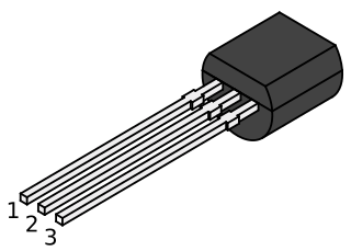
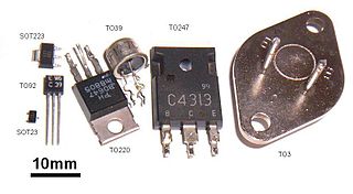
The TO-92 is a widely used style of semiconductor package mainly used for transistors. The case is often made of epoxy or plastic, and offers compact size at a very low cost.

<span class="mw-page-title-main">TO-220</span> Power semiconductor through-hole package

The TO-220 is a style of electronic package used for high-powered, through-hole components with 0.1 inches (2.54 mm) pin spacing. The "TO" designation stands for "transistor outline". TO-220 packages have three leads. Similar packages with two, four, five or seven leads are also manufactured. A notable characteristic is a metal tab with a hole, used to mount the case to a heatsink, allowing the component to dissipate more heat than one constructed in a TO-92 case. Common TO-220-packaged components include discrete semiconductors such as transistors and silicon-controlled rectifiers, as well as integrated circuits.

<span class="mw-page-title-main">TO-3</span> Metal can semiconductor package for power semiconductors

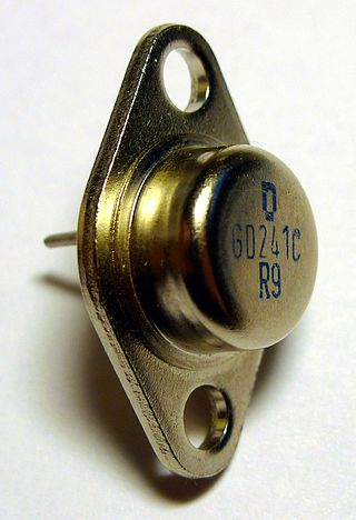
In electronics, TO-3 is a designation for a standardized metal semiconductor package used for power semiconductors, including transistors, silicon controlled rectifiers, and, integrated circuits. TO stands for "Transistor Outline" and relates to a series of technical drawings produced by JEDEC.

<span class="mw-page-title-main">2N3904</span> Common NPN bipolar junction transistor

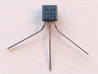
The 2N3904 is a common NPN bipolar junction transistor used for general-purpose low-power amplifying or switching applications. It is designed for low current and power, medium voltage, and can operate at moderately high speeds. It is complementary to the 2N3906 PNP transistor. Both types were registered by Motorola Semiconductor in the mid-1960s.

<span class="mw-page-title-main">1N4148 signal diode</span> Standard silicon switching diode

The 1N4148 is a standard silicon switching signal diode. It is one of the most popular and long-lived switching diodes because of its dependable specifications and low cost. Its name follows the JEDEC nomenclature. The 1N4148 is useful in switching applications up to about 100 MHz with a reverse-recovery time of no more than 4 ns.

The JEDEC memory standards are the specifications for semiconductor memory circuits and similar storage devices promulgated by the Joint Electron Device Engineering Council (JEDEC) Solid State Technology Association, a semiconductor trade and engineering standardization organization.

<span class="mw-page-title-main">BC548</span>

The BC548 is a general-purpose NPN bipolar junction transistor commonly used in European and American electronic equipment. It is notably often the first type of bipolar transistor hobbyists encounter and is often featured in designs in hobby electronics magazines where a general-purpose transistor is required. The BC548 is low in cost and widely available.

A semiconductor package is a metal, plastic, glass, or ceramic casing containing one or more discrete semiconductor devices or integrated circuits. Individual components are fabricated on semiconductor wafers before being diced into die, tested, and packaged. The package provides a means for connecting it to the external environment, such as printed circuit board, via leads such as lands, balls, or pins; and protection against threats such as mechanical impact, chemical contamination, and light exposure. Additionally, it helps dissipate heat produced by the device, with or without the aid of a heat spreader. There are thousands of package types in use. Some are defined by international, national, or industry standards, while others are particular to an individual manufacturer.

<span class="mw-page-title-main">TO-18</span>

In electronics, TO-18 is a designation for a style of transistor metal case. The case is more expensive than the similarly sized plastic TO-92 package. The name is from JEDEC, signifying Transistor Outline Package, Case Style 18.

<span class="mw-page-title-main">DO-204</span>

DO-204 is a family of diode semiconductor packages defined by JEDEC. This family comprises lead-mounted axial devices with round leads. Generally a diode will have a line painted near the cathode end.

<span class="mw-page-title-main">TO-263</span> Surface mount power semiconductor package

The Double Decawatt Package, D2PAK, SOT404 or DDPAK, standardized as TO-263, is a semiconductor package type intended for surface mounting on circuit boards. The TO-263 is designed by Motorola. They are similar to the earlier TO-220-style packages intended for high power dissipation but lack the extended metal tab and mounting hole, while representing a larger version of the TO-252, also known as DPAK, SMT package. As with all SMT packages, the pins on a D2PAK are bent to lie against the PCB surface. The TO-263 can have 3 to 7 terminals.

<span class="mw-page-title-main">Small-outline transistor</span> Family of discrete surface mount transistors

A small outline transistor (SOT) is a family of small footprint, discrete surface mount transistor commonly used in consumer electronics. The most common SOT are SOT23 variations,. SOT23-5 differs from SOT23 in a wider body of 1.6 mm (0.063 in) instead of 1.3 mm (0.051 in). Also, manufacturers offer the nearly identical thin small outline transistor (TSOT/TSOP) package, where lower height is important.

<span class="mw-page-title-main">TO-126</span>

TO-126 is a type of semiconductor package for devices with three pins, such as transistors. The package is rectangular with a hole in the middle to allow for easy mounting to a board or a heat sink. On one side of the package typically a metal sheet is exposed, with the transistor die bonded to the other side of the metal sheet inside the package. This allows for an efficient heat transfer from the transistor die to an external heat sink but also implies that the metal sheet is electrically connected to the die.

<span class="mw-page-title-main">TO-66</span> Smaller variant of the TO-3 package

TO-66 is a type of semiconductor package for devices with three connections, such as transistors. The shape is similar to the TO-3 package, but the size is smaller. The TO-66 package is made entirely of metal and is commonly used by silicon controlled rectifiers and power transistors. In Europe, it was popularly used by the complementary germanium power transistors AD161/AD162.

<span class="mw-page-title-main">TO-8</span>

In electronics, TO-8 is a designation for a standardized metal semiconductor package. TO in TO-8 stands for "transistor outline" and refers to a series of technical drawings produced by JEDEC. The TO-8 package is noticeably larger than the more common TO-5 package. While originally designed for medium power transistors such as the 2N1483 series or the AD136, it is more commonly used for integrated circuits and sensors.

References

  1. 1 2 "JEDEC TO-5 package specification" (PDF). JEDEC . Archived from the original (PDF) on June 18, 2017.
  2. 1 2 "Fairchild 2N697". Transistor Museum. Retrieved 2021-07-16.
  3. "Metal Can Packages" (PDF). National Semiconductor / Texas Instruments. August 1999. pp. 7–14. Retrieved 2021-06-21.
  4. "1965: Package is the first to accommodate system design considerations". Computer History Museum. Retrieved 2021-06-21.
  5. "TO-39" (PDF). JEDEC. Archived from the original (PDF) on 2016-04-10. Retrieved 2021-06-21.
  6. "TO-9" (PDF). JEDEC. Archived from the original (PDF) on 2016-04-10. Retrieved 2021-06-21.
  7. "...does not meet the minimum criteria ...for registration." "TO-42" (PDF). JEDEC. Archived from the original (PDF) on 2016-04-05. Retrieved 2021-06-21.
  8. "TO-12" (PDF). JEDEC. Archived from the original (PDF) on 2016-04-05. Retrieved 2021-06-21.
  9. "TO-33" (PDF). JEDEC. Archived from the original (PDF) on 2016-04-04. Retrieved 2021-06-21.
  10. "TO-75" (PDF). JEDEC. Archived from the original (PDF) on 2016-04-05. Retrieved 2021-06-21.
  11. "TO-76" (PDF). JEDEC. Archived from the original (PDF) on 2016-04-04. Retrieved 2021-06-21.
  12. "TO-77" (PDF). JEDEC. Archived from the original (PDF) on 2016-04-05. Retrieved 2021-06-21.
  13. "TO-78" (PDF). JEDEC. Archived from the original (PDF) on 2016-04-05. Retrieved 2021-06-21.
  14. "TO-79" (PDF). JEDEC. Archived from the original (PDF) on 2016-04-10. Retrieved 2021-06-21.
  15. "TO-80" (PDF). JEDEC. Archived from the original (PDF) on 2016-04-05. Retrieved 2021-06-21.
  16. "TO-99" (PDF). JEDEC. Archived from the original (PDF) on 2016-04-10. Retrieved 2021-06-21.
  17. "TO-74" (PDF). JEDEC. Archived from the original (PDF) on 2016-04-10. Retrieved 2021-06-21.
  18. "TO-96" (PDF). JEDEC. Archived from the original (PDF) on 2016-04-10. Retrieved 2021-06-21.
  19. "TO-97" (PDF). JEDEC. Archived from the original (PDF) on 2016-04-05. Retrieved 2021-06-21.
  20. "TO-100" (PDF). JEDEC. Archived from the original (PDF) on 2016-04-10. Retrieved 2021-06-21.
  21. "TO-73" (PDF). JEDEC. Archived from the original (PDF) on 2016-04-10. Retrieved 2021-06-21.
  22. "TO-101" (PDF). JEDEC. Archived from the original (PDF) on 2016-04-10. Retrieved 2021-06-21.
  23. "Index by Device Type of Registered Transistor Outlines (TO)". JEDEC Publication No. 95 (PDF). JEDEC. October 2010. Retrieved 2021-07-13.
  24. 1 2 "Header Family 0.200 Pin Circle". JEDEC Publication No. 95 (PDF). JEDEC. November 1982. pp. 178–181. Retrieved 2021-07-13.
  25. 1 2 3 "Semiconductors" (PDF). Pro Electron. 1978. pp. 215–219. Retrieved 2021-06-17.
  26. "Semiconductor Databook" (PDF). Heilbronn: AEG-Telefunken. p. 15. Retrieved 2021-08-20.
  27. "EIAJ ED-7500A Standards for the Dimensions of Semiconductor Devices" (PDF). JEITA. 1996. Retrieved 2021-06-14.
  28. "Semiconductor and Photoelectric Devices" (PDF). Mullard. 1968. p. 457. Retrieved 2021-06-14.
  29. "ГОСТ 18472—88 ПРИБОРЫ ПОЛУПРОВОДНИКОВЫЕ - Основные размеры" [GOST 18472—88 Semiconductor devices - basic dimensions](PDF) (in Russian). Rosstandart. 1988. pp. 37–38. Retrieved 2021-06-17.
  30. "ПРИБОРЫ ПОЛУПРОВОДНИКОВЫЕ - Основные размеры" [Semiconductor devices - basic dimensions](PDF) (in Russian). Rosstandart. 2017. p. 45. Retrieved 2021-06-17.
  31. 1 2 "TGL 26713/07: Gehäuse für Halbleiterbauelemente - Bauform F" (PDF) (in German). Leipzig: Verlag für Standardisierung. June 1988. Retrieved 2021-06-15.