An integrated circuit or monolithic integrated circuit is a set of electronic circuits on one small flat piece of semiconductor material, usually silicon. Large numbers of miniaturized transistors and other electronic components are integrated together on the chip. This results in circuits that are orders of magnitude smaller, faster, and less expensive than those constructed of discrete components, allowing a large transistor count. The IC's mass production capability, reliability, and building-block approach to integrated circuit design have ensured the rapid adoption of standardized ICs in place of designs using discrete transistors. ICs are now used in virtually all electronic equipment and have revolutionized the world of electronics. Computers, mobile phones and other home appliances are now inextricable parts of the structure of modern societies, made possible by the small size and low cost of ICs such as modern computer processors and microcontrollers.

Semiconductor device fabrication is the process used to manufacture semiconductor devices, typically integrated circuits (ICs) such as computer processors, microcontrollers, and memory chips that are present in everyday electrical and electronic devices. It is a multiple-step photolithographic and physio-chemical process during which electronic circuits are gradually created on a wafer, typically made of pure single-crystal semiconducting material. Silicon is almost always used, but various compound semiconductors are used for specialized applications.

A ball grid array (BGA) is a type of surface-mount packaging used for integrated circuits. BGA packages are used to permanently mount devices such as microprocessors. A BGA can provide more interconnection pins than can be put on a dual in-line or flat package. The whole bottom surface of the device can be used, instead of just the perimeter. The traces connecting the package's leads to the wires or balls which connect the die to package are also on average shorter than with a perimeter-only type, leading to better performance at high speeds.

Flip chip, also known as controlled collapse chip connection or its abbreviation, C4, is a method for interconnecting dies such as semiconductor devices, IC chips, integrated passive devices and microelectromechanical systems (MEMS), to external circuitry with solder bumps that have been deposited onto the chip pads. The technique was developed by General Electric's Light Military Electronics Department, Utica, New York. The solder bumps are deposited on the chip pads on the top side of the wafer during the final wafer processing step. In order to mount the chip to external circuitry, it is flipped over so that its top side faces down, and aligned so that its pads align with matching pads on the external circuit, and then the solder is reflowed to complete the interconnect. This is in contrast to wire bonding, in which the chip is mounted upright and fine wires are welded onto the chip pads and lead frame contacts to interconnect the chip pads to external circuitry.

In electronics manufacturing, integrated circuit packaging is the final stage of semiconductor device fabrication, in which the block of semiconductor material is encapsulated in a supporting case that prevents physical damage and corrosion. The case, known as a "package", supports the electrical contacts which connect the device to a circuit board.

A chip scale package or chip-scale package (CSP) is a type of integrated circuit package.
Wafer-scale integration (WSI) is a rarely used system of building very-large integrated circuit networks from an entire silicon wafer to produce a single "super-chip". Combining large size and reduced packaging, WSI was expected to lead to dramatically reduced costs for some systems, notably massively parallel supercomputers. The name is taken from the term very-large-scale integration, the state of the art when WSI was being developed.
In electronics, a lead is an electrical connection consisting of a length of wire or a metal pad that is designed to connect two locations electrically. Leads are used for many purposes, including: transfer of power; testing of an electrical circuit to see if it is working, using a test light or a multimeter; transmitting information, as when the leads from an electrocardiograph are attached to a person's body to transmit information about their heart rhythm; and sometimes to act as a heatsink. The tiny leads coming off through-hole electronic components are also often called pins; in ball grid array packages, they are in form of small spheres, and are therefore called "balls".

The back end of line (BEOL) is the second portion of IC fabrication where the individual devices get interconnected with wiring on the wafer, the metalization layer. Common metals are copper and aluminum. BEOL generally begins when the first layer of metal is deposited on the wafer. BEOL includes contacts, insulating layers (dielectrics), metal levels, and bonding sites for chip-to-package connections.

International Rectifier was an American power management technology company manufacturing analog and mixed-signal ICs, advanced circuit devices, integrated power systems, and high-performance integrated components for computing. On 13 January 2015, the company became a part of Infineon Technologies.

Flat no-leads packages such as quad-flat no-leads (QFN) and dual-flat no-leads (DFN) physically and electrically connect integrated circuits to printed circuit boards. Flat no-leads, also known as micro leadframe (MLF) and SON, is a surface-mount technology, one of several package technologies that connect ICs to the surfaces of PCBs without through-holes. Flat no-lead is a near chip scale plastic encapsulated package made with a planar copper lead frame substrate. Perimeter lands on the package bottom provide electrical connections to the PCB. Flat no-lead packages usually, but not always, include an exposed thermally conductive pad to improve heat transfer out of the IC. Heat transfer can be further facilitated by metal vias in the thermal pad. The QFN package is similar to the quad-flat package (QFP), and a ball grid array (BGA).
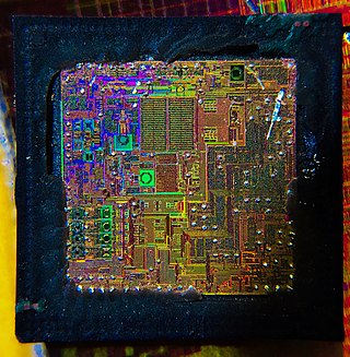
A die, in the context of integrated circuits, is a small block of semiconducting material on which a given functional circuit is fabricated. Typically, integrated circuits are produced in large batches on a single wafer of electronic-grade silicon (EGS) or other semiconductor through processes such as photolithography. The wafer is cut (diced) into many pieces, each containing one copy of the circuit. Each of these pieces is called a die.

Bahgat G. Sammakia is an educator and academic administrator who currently serves as Vice President for Research at Binghamton University. He was previously the Interim President of the SUNY Polytechnic Institute. He is also a professor of mechanical engineering and director of the Small Scale Systems Packaging Center at Binghamton University in Binghamton, New York. Sammakia has published over 200 technical papers in refereed journals and conference proceedings, holds 21 U.S. patents and 12 IBM technical disclosures. He has also contributed to three books.

In electronic engineering, a through-silicon via (TSV) or through-chip via is a vertical electrical connection (via) that passes completely through a silicon wafer or die. TSVs are high-performance interconnect techniques used as an alternative to wire-bond and flip chips to create 3D packages and 3D integrated circuits. Compared to alternatives such as package-on-package, the interconnect and device density is substantially higher, and the length of the connections becomes shorter.
A three-dimensional integrated circuit is a MOS integrated circuit (IC) manufactured by stacking as many as 16 or more ICs and interconnecting them vertically using, for instance, through-silicon vias (TSVs) or Cu-Cu connections, so that they behave as a single device to achieve performance improvements at reduced power and smaller footprint than conventional two dimensional processes. The 3D IC is one of several 3D integration schemes that exploit the z-direction to achieve electrical performance benefits in microelectronics and nanoelectronics.
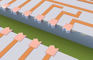
Quilt Packaging (QP) is an integrated circuit packaging and chip-to-chip interconnect packaging technology that utilizes “nodule” structures that extend out horizontally from the edges of microchips to make electrically and mechanically robust chip-to-chip interconnections.

Wafer-level packaging (WLP) is a process where packaging components are attached to an integrated circuit (IC) before the wafer – on which the IC is fabricated – is diced. In WSP, the top and bottom layers of the packaging and the solder bumps are attached to the integrated circuits while they are still in the wafer. This process differs from a conventional process, in which the wafer is sliced into individual circuits (dice) before the packaging components are attached.

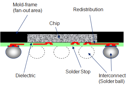
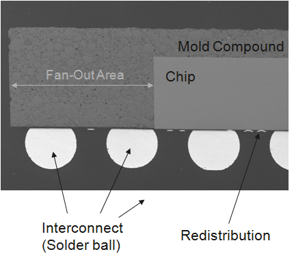
Fan-out wafer-level packaging is an integrated circuit packaging technology, and an enhancement of standard wafer-level packaging (WLP) solutions.
Glossary of microelectronics manufacturing terms