Wire wrap

Last updated
Close-up of a wire-wrap connection Wire Wrapping.jpg
Close-up of a wire-wrap connection
Typical wire wrap construction of Bell System telephone crossbar switch. Some types of connection were soldered. Crossbar-banjo1-hy.jpg
Typical wire wrap construction of Bell System telephone crossbar switch. Some types of connection were soldered.

Wire wrap is an electronic component assembly technique that was invented to wire telephone crossbar switches, and later adapted to construct electronic circuit boards. Electronic components mounted on an insulating board are interconnected by lengths of insulated wire run between their terminals, with the connections made by wrapping several turns of uninsulated sections of the wire around a component lead or a socket pin.

Contents

Wires can be wrapped by hand or by machine, and can be hand-modified afterwards. It was popular for large-scale manufacturing in the 1960s and early 1970s, and continues today to be used for short runs and prototypes. The method eliminates the design and fabrication of a printed circuit board. Wire wrapping is unusual among other prototyping technologies since it allows for complex assemblies to be produced by automated equipment, but then easily repaired or modified by hand.

Wire wrap construction can produce assemblies that are more reliable than printed circuits: connections are less prone to fail due to vibration or physical stresses on the base board, and the lack of solder eliminates soldering faults such as corrosion, cold joints and dry joints. The connections themselves are firmer and have lower electrical resistance due to cold welding of the wire to the terminal post at the corners.

Wire wrap was used for assembly of high frequency prototypes and small production runs, including gigahertz microwave circuits and supercomputers. It is unique among automated prototyping techniques in that wire lengths can be exactly controlled, and twisted pairs or magnetically shielded twisted quads can be routed together.

Wire wrap construction became popular around 1960 in circuit board manufacturing, and use has now sharply declined. Surface-mount technology has made the technique much less useful than in previous decades. Solder-less breadboards and the decreasing cost of professionally made PCBs have nearly eliminated this technology.

History

Wire wrapped backplane of an IBM 1401 computer, introduced in 1959 IBM 1401 backplane.jpg
Wire wrapped backplane of an IBM 1401 computer, introduced in 1959
A modern wire wrap in a CFL Wire wrap in OSRAM CFL.jpg
A modern wire wrap in a CFL

Manually wrapped wires were common in early 20th century point-to-point electronic construction methods in which a strong connection was needed to hold the components in place. Wires were wrapped by hand around binding posts or spade lugs and then soldered.

Modern wire wrapping technology was developed after WWII at Bell Laboratories as a means of making electrical connections in a new relay being designed for use in the Bell Telephone system. [1] A design team headed by Arthur C. Keller developed the “Keller Wrap Gun”, and the entire wrap system was passed over to Western Electric for industrial application. After a “make or buy” committee at Western Electric decided to have the hand tool manufactured by an outside vendor, Western Electric sent the tool contract out for bids. Keller Tool of Grand Haven, Michigan, a supplier of rotary hand tools to Western Electric, won the contract and made several design changes to make the tool easier to manufacture and to use. Keller began manufacturing the tools in 1953, and subsequently obtained a license from Western Electric allowing sale of the technology on the open market. The tool was marketed under its original name – since the name of the manufacturer was coincidentally the same as the name of the inventor.

IBM's first transistorized computers, introduced within the late 1950s, were built with the IBM Standard Modular System that used wire-wrapped backplanes.

Wire-wrap was used by Apple Computer to make early prototypes of the original Macintosh computer (The Macintosh 128K). [2]

Method

Manual wire wrapping/stripping tool Manual wire wrap tool and wire wrap wire in various colours.jpg
Manual wire wrapping/stripping tool

A correctly made wire-wrap connection for 30 or 28 AWG wire is seven turns (fewer for larger wire) of bare wire with half to one and a half turns of insulated wire at the bottom for strain relief. [3] [4] The square hard-gold-plated post thus forms 28 redundant contacts. The silver-plated wire coating cold-welds to the gold. If corrosion occurs, it occurs on the outside of the wire, not on the gas-tight contact where oxygen cannot penetrate to form oxides. A correctly designed wire-wrap tool applies up to twenty tons of force per square inch on each joint.

The electronic parts sometimes plug into sockets. The sockets are attached with cyanoacrylate (or silicone adhesive) to thin plates of glass-fiber-reinforced epoxy (fiberglass).

The sockets have square posts. The usual posts are 0.025 in (0.64 mm) square, 1 in (25.4 mm) high, and spaced at 0.1 in (2.54 mm) intervals. Premium posts are hard-drawn beryllium copper alloy plated with a 0.000025 in (630 nm) of gold to prevent corrosion. Less-expensive posts are bronze with tin plating.

30 gauge (~0.0509mm2) silver-plated soft copper wire is insulated with a fluorocarbon that does not emit dangerous gases when heated. The most common insulation is "Kynar". The 30 AWG Kynar wire is cut into standard lengths, then one inch of insulation is removed on each end.

There are three ways of placing wires on a board. In professionally built wire-wrap boards, long wires are placed first so that shorter wires mechanically secure the long wires. Also, to make an assembly more repairable, wires are applied in layers. The ends of each wire are always at the same height on the post, so that at most three wires need to be replaced to replace a wire. Also, to make the layers easier to see, they are made with different colors of insulation. In space-rated or airworthy wire-wrap assemblies, the wires are boxed, and may be conformally coated with wax to reduce vibration. Epoxy is never used for the coating because it makes an assembly unrepairable.[ citation needed ]

Tooling

Mechanical wire wrap tool MechanicalWrapGun.png
Mechanical wire wrap tool
Electrical wire wrap tool; pneumatic (air-powered) tools are also available WrapGun.png
Electrical wire wrap tool; pneumatic (air-powered) tools are also available

A "wire wrap tool" has two holes. The wire and 14 in (6.4 mm) of insulated wire are placed in a hole near the edge of the tool. The hole in the center of the tool is placed over the post.

The tool is rapidly twisted. The result is that 1.5 to 2 turns of insulated wire are wrapped around the post, and above that, 7 to 9 turns of bare wire are wrapped around the post. The post has room for three such connections, although usually only one or two are needed. This facilitates manual wire-wrapping to be employed for modifications or repairs.

The turn and a half of insulated wire helps prevent wire fatigue where it meets the post.

Above the turn of insulated wire, the bare wire wraps around the post. The corners of the post bite in with pressures of tons per square inch. This forces all the gases out of the area between the wire's silver plate and the post's gold or tin corners. Further, with 28 such connections (seven turns on a four-cornered post), a very reliable connection exists between the wire and the post. Furthermore, the corners of the posts are quite "sharp": they have a quite-small radius of curvature.[ citation needed ]

Automation

The two holes at the end of a manual wire wrap tool. The wire goes in the one near the edge, and the post is inserted into the hole in the center Wire wrap tool.jpg
The two holes at the end of a manual wire wrap tool. The wire goes in the one near the edge, and the post is inserted into the hole in the center

Automated wire-wrap machines, as manufactured by the Gardner Denver Company in the 1960s and 1970s, were capable of automatically routing, cutting, stripping and wrapping wires onto an electronic "backplane" or "circuit board". The machines were driven by wiring instructions encoded onto punched cards, [5] Mylar punched hole tape, and early micro computers.

The earliest machines (14FB and 14FG models, for example) were initially configured as "horizontal", which meant that the wire wrap board was placed upside down (pins up) onto a horizontal tooling plate, which was then rolled into the machine and locked onto a rotating (TRP table rotational position of four positions) and shifting (PLP = pallet longitudinal position of 11 positions) pallet assembly. These machines included very large hydraulic units for powering the servos that drove the ball screw mounted "A" and "B" drive carriages, a 6 ft (1.8 m) tall electronics cabinet loaded with hundreds of IBM control relays, many dozens of solenoids for controlling the various pneumatic mechanical subsystems, and an IBM 029 card reader for positioning instructions. The automatic wire wrap machines themselves were quite large, 6 ft (1.8 m) tall and 8 ft (2.4 m) square. Servicing the machines was extremely complex, and often meant climbing inside them just to work on them. This could be quite dangerous if safety interlocks were not maintained properly.

Later, somewhat smaller machines were "vertical" (14FV) which meant the boards were placed onto a tooling plate with pins facing the machine operator. Gone were the hydraulic units, in favor of direct drive motors to rotate the ball screws, with rotary encoders to provide positioning feedback. This generally provided better visibility of the product for the operator, although maximum wrap area was significantly less than the horizontal machines. Top speeds on horizontal machines were generally around 500-600 wires per hour, while the vertical machines could reach rates as high as 1200 per hour, depending on board quality and wiring configurations.

Considerations

Wire-wrap works well with digital circuits with few discrete components, but is less convenient for analog systems with many discrete resistors, capacitors or other components (such elements can be soldered to a header and plugged into a wire wrap socket). [6] The sockets are an additional cost compared to directly inserting integrated circuits into a printed circuit board, and add size and mass to a system. Multiple strands of wire may introduce cross-talk between circuits, of little consequence for digital circuits but a limitation for analog systems. The interconnected wires can radiate electromagnetic interference and have less predictable impedance than a printed circuit board. Wire-wrap construction cannot provide the ground planes and power distribution planes possible with multilayer printed circuit boards, increasing the possibility of noise. [7]

See also

Related Research Articles

<span class="mw-page-title-main">Dual in-line package</span> Type of electronic component package

In microelectronics, a dual in-line package is an electronic component package with a rectangular housing and two parallel rows of electrical connecting pins. The package may be through-hole mounted to a printed circuit board (PCB) or inserted in a socket. The dual-inline format was invented by Don Forbes, Rex Rice and Bryant Rogers at Fairchild R&D in 1964, when the restricted number of leads available on circular transistor-style packages became a limitation in the use of integrated circuits. Increasingly complex circuits required more signal and power supply leads ; eventually microprocessors and similar complex devices required more leads than could be put on a DIP package, leading to development of higher-density chip carriers. Furthermore, square and rectangular packages made it easier to route printed-circuit traces beneath the packages.

<span class="mw-page-title-main">Printed circuit board</span> Board to support and connect electronic components

A printed circuit board (PCB), also called printed wiring board (PWB), is a medium used to connect or "wire" components to one another in a circuit. It takes the form of a laminated sandwich structure of conductive and insulating layers: each of the conductive layers is designed with a pattern of traces, planes and other features etched from one or more sheet layers of copper laminated onto and/or between sheet layers of a non-conductive substrate. Electrical components may be fixed to conductive pads on the outer layers in the shape designed to accept the component's terminals, generally by means of soldering, to both electrically connect and mechanically fasten them to it. Another manufacturing process adds vias, plated-through holes that allow interconnections between layers.

<span class="mw-page-title-main">Point-to-point construction</span> Making an electronic circuit by directly connecting the leads of the components

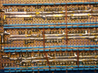
In electronics, point-to-point construction is a non-automated technique for constructing circuits which was widely used before the use of printed circuit boards (PCBs) and automated assembly gradually became widespread following their introduction in the 1950s. Circuits using thermionic valves were relatively large, relatively simple, and used large sockets, all of which made the PCB less obviously advantageous than with later complex semiconductor circuits. Point-to-point construction is still widespread in power electronics, where components are bulky and serviceability is a consideration, and to construct prototype equipment with few or heavy electronic components. A common practice, especially in older point-to-point construction, is to use the leads of components such as resistors and capacitors to bridge as much of the distance between connections as possible, reducing the need to add additional wire between the components.

<span class="mw-page-title-main">Breadboard</span> Board with embedded spring clips that allows for electronics to be wired without soldering

A breadboard, solderless breadboard, or protoboard is a construction base used to build semi-permanent prototypes of electronic circuits. Unlike a perfboard or stripboard, breadboards do not require soldering or destruction of tracks and are hence reusable. For this reason, breadboards are also popular with students and in technological education.

<span class="mw-page-title-main">Electrical connector</span> Device used to join electrical conductors

Components of an electrical circuit are electrically connected if an electric current can run between them through an electrical conductor. An electrical connector is an electromechanical device used to create an electrical connection between parts of an electrical circuit, or between different electrical circuits, thereby joining them into a larger circuit. Most electrical connectors have a gender – i.e. the male component, called a plug, connects to the female component, or socket. The connection may be removable, require a tool for assembly and removal, or serve as a permanent electrical joint between two points. An adapter can be used to join dissimilar connectors.

<span class="mw-page-title-main">Surface-mount technology</span> Method for producing electronic circuits

Surface-mount technology (SMT), originally called planar mounting, is a method in which the electrical components are mounted directly onto the surface of a printed circuit board (PCB). An electrical component mounted in this manner is referred to as a surface-mount device (SMD). In industry, this approach has largely replaced the through-hole technology construction method of fitting components, in large part because SMT allows for increased manufacturing automation which reduces cost and improves quality. It also allows for more components to fit on a given area of substrate. Both technologies can be used on the same board, with the through-hole technology often used for components not suitable for surface mounting such as large transformers and heat-sinked power semiconductors.

<span class="mw-page-title-main">Stripboard</span>

Stripboard is the generic name for a widely used type of electronics prototyping material for circuit boards characterized by a pre-formed 0.1 inches (2.54 mm) regular (rectangular) grid of holes, with wide parallel strips of copper cladding running in one direction all the way across one side of on an insulating bonded paper board. It is commonly also known by the name of the original product Veroboard, which is a trademark, in the UK, of British company Vero Technologies Ltd and Canadian company Pixel Print Ltd. It was originated and developed in the early 1960s by the Electronics Department of Vero Precision Engineering Ltd (VPE). It was introduced as a general-purpose material for use in constructing electronic circuits - differing from purpose-designed printed circuit boards (PCBs) in that a variety of electronics circuits may be constructed using a standard wiring board.

<span class="mw-page-title-main">Flip chip</span> Technique that flips a microchip upside down to connect it

Flip chip, also known as controlled collapse chip connection or its abbreviation, C4, is a method for interconnecting dies such as semiconductor devices, IC chips, integrated passive devices and microelectromechanical systems (MEMS), to external circuitry with solder bumps that have been deposited onto the chip pads. The technique was developed by General Electric's Light Military Electronics Department, Utica, New York. The solder bumps are deposited on the chip pads on the top side of the wafer during the final wafer processing step. In order to mount the chip to external circuitry, it is flipped over so that its top side faces down, and aligned so that its pads align with matching pads on the external circuit, and then the solder is reflowed to complete the interconnect. This is in contrast to wire bonding, in which the chip is mounted upright and fine wires are welded onto the chip pads and lead frame contacts to interconnect the chip pads to external circuitry.

<span class="mw-page-title-main">D-subminiature</span> Type of electrical connector

The D-subminiature or D-sub is a common type of electrical connector. They are named for their characteristic D-shaped metal shield. When they were introduced, D-subs were among the smallest connectors used on computer systems.

<span class="mw-page-title-main">Through-hole technology</span> Circuit board manufacturing technique

In electronics, through-hole technology is a manufacturing scheme in which leads on the components are inserted through holes drilled in printed circuit boards (PCB) and soldered to pads on the opposite side, either by manual assembly or by the use of automated insertion mount machines.

<span class="mw-page-title-main">Wiring pencil</span>

A wiring pencil is a tool for making electrical connections.

<span class="mw-page-title-main">Perfboard</span> Material for prototyping electronic circuits

Perfboard is a material for prototyping electronic circuits. It is a thin, rigid sheet with holes pre-drilled at standard intervals across a grid, usually a square grid of 0.1 inches (2.54 mm) spacing. These holes are ringed by round or square copper pads, though bare boards are also available. Inexpensive perfboard may have pads on only one side of the board, while better quality perfboard can have pads on both sides. Since each pad is electrically isolated, the builder makes all connections with either wire wrap or miniature point to point wiring techniques. Discrete components are soldered to the prototype board such as resistors, capacitors, and integrated circuits. The substrate is typically made of paper laminated with phenolic resin or a fiberglass-reinforced epoxy laminate (FR-4).

Electronic packaging is the design and production of enclosures for electronic devices ranging from individual semiconductor devices up to complete systems such as a mainframe computer. Packaging of an electronic system must consider protection from mechanical damage, cooling, radio frequency noise emission and electrostatic discharge. Product safety standards may dictate particular features of a consumer product, for example, external case temperature or grounding of exposed metal parts. Prototypes and industrial equipment made in small quantities may use standardized commercially available enclosures such as card cages or prefabricated boxes. Mass-market consumer devices may have highly specialized packaging to increase consumer appeal. Electronic packaging is a major discipline within the field of mechanical engineering.

<span class="mw-page-title-main">Turret board</span> Early electronic circuit board design

In electronics, turret boards were an early attempt at making circuits that were relatively rugged, producible, and serviceable in the days before printed circuit boards (PCBs). As this method was somewhat more expensive than conventional "point-to-point" wiring techniques, it was generally found in the more expensive components, such as professional, commercial, and military audio and test equipment. This is similar to cordwood construction.

<span class="mw-page-title-main">Screw terminal block</span> Device for electrical wire connection

A screw terminal is a type of electrical connection where a wire is held by the tightening of a screw.

A semiconductor package is a metal, plastic, glass, or ceramic casing containing one or more discrete semiconductor devices or integrated circuits. Individual components are fabricated on semiconductor wafers before being diced into die, tested, and packaged. The package provides a means for connecting it to the external environment, such as printed circuit board, via leads such as lands, balls, or pins; and protection against threats such as mechanical impact, chemical contamination, and light exposure. Additionally, it helps dissipate heat produced by the device, with or without the aid of a heat spreader. There are thousands of package types in use. Some are defined by international, national, or industry standards, while others are particular to an individual manufacturer.

Speedwire is a solderless prototyping system manufactured by BICC-Vero for constructing electronic circuit boards. The system is based on a circuit board pre-drilled with holes in a regular 0.1-inch square grid. The boards are available in standard sizes such as Eurocard modules. Some of the holes are through-plated and interconnected with copper strips to form power and ground rails.

<span class="mw-page-title-main">Chip carrier</span> Surface mount technology package for integrated circuits

In electronics, a chip carrier is one of several kinds of surface-mount technology packages for integrated circuits. Connections are made on all four edges of a square package; compared to the internal cavity for mounting the integrated circuit, the package overall size is large.

<span class="mw-page-title-main">Chip on board</span> Method of circuit board manufacture

Chip on board (COB) is a method of circuit board manufacturing in which the integrated circuits (e.g. microprocessors) are attached (wired, bonded directly) to a printed circuit board, and covered by a blob of epoxy. By eliminating the packaging of individual semiconductor devices, the completed product can be more compact, lighter, and less costly. In some cases, COB construction improves the operation of radio frequency systems by reducing the inductance and capacitance of integrated circuit leads.

<span class="mw-page-title-main">Electronics prototyping</span>

In electronics, prototyping means building an actual circuit to a theoretical design to verify that it works, and to provide a physical platform for debugging it if it does not. The prototype is often constructed using techniques such as wire wrapping or using a breadboard, stripboard or perfboard, with the result being a circuit that is electrically identical to the design but not physically identical to the final product.

References

  1. Bell Telephone Laboratories (1953). "A New Twist in Telephony (advertisement)" . Retrieved November 3, 2018.
  2. "Hello. The Apple Mac @ 40". CHM. Archived from the original on January 22, 2024. Retrieved 2024-01-24.
  3. "Standards for Discrete Wiring", Workmanship, USA: NASA, 2000-03-31, retrieved 2011-08-21
  4. Department of Defense (12 December 1978). "Military Standard: Connections, Electrical, Solderless Wrapped" (pdf). sec. 5.3.2. Retrieved 2016-11-04.
  5. Horowitz and Hill, "The Art of Electronics 3rd Edition", pp. 828-830
  6. Horowitz and Hill "the Art of Electronics 3rd Edition", p. 816