
The GeForce FX or "GeForce 5" series is a line of graphics processing units from the manufacturer Nvidia.

The GeForce 2 series (NV15) is the second generation of Nvidia's GeForce line of graphics processing units (GPUs). Introduced in 2000, it is the successor to the GeForce 256.

The GeForce 4 series refers to the fourth generation of Nvidia's GeForce line of graphics processing units (GPUs). There are two different GeForce4 families, the high-performance Ti family, and the budget MX family. The MX family spawned a mostly identical GeForce4 Go (NV17M) family for the laptop market. All three families were announced in early 2002; members within each family were differentiated by core and memory clock speeds. In late 2002, there was an attempt to form a fourth family, also for the laptop market, the only member of it being the GeForce4 4200 Go (NV28M) which was derived from the Ti line.

The RIVA 128, or "NV3", was a consumer graphics processing unit created in 1997 by Nvidia. It was the first to integrate 3D acceleration in addition to traditional 2D and video acceleration. Its name is an acronym for Real-time Interactive Video and Animation accelerator.

The GeForce 6 series is the sixth generation of Nvidia's GeForce line of graphics processing units. Launched on April 14, 2004, the GeForce 6 family introduced PureVideo post-processing for video, SLI technology, and Shader Model 3.0 support.
The R420 GPU, developed by ATI Technologies, was the company's basis for its 3rd-generation DirectX 9.0/OpenGL 2.0-capable graphics cards. Used first on the Radeon X800, the R420 was produced on a 0.13 micrometer low-K photolithography process and used GDDR-3 memory. The chip was designed for AGP graphics cards.

The Voodoo 5 was the last and most powerful graphics card line that was released by 3dfx Interactive. All members of the family were based upon the VSA-100 graphics processor. Only the single-chip Voodoo 4 4500 and dual-chip Voodoo 5 5500 made it to market.

Savage was a product-line of PC graphics chipsets designed by S3.
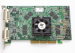
The R200 is the second generation of GPUs used in Radeon graphics cards and developed by ATI Technologies. This GPU features 3D acceleration based upon Microsoft Direct3D 8.1 and OpenGL 1.3, a major improvement in features and performance compared to the preceding Radeon R100 design. The GPU also includes 2D GUI acceleration, video acceleration, and multiple display outputs. "R200" refers to the development codename of the initially released GPU of the generation. It is the basis for a variety of other succeeding products.

The GeForce 7 series is the seventh generation of Nvidia's GeForce line of graphics processing units. This was the last series available on AGP cards.
The R520 is a graphics processing unit (GPU) developed by ATI Technologies and produced by TSMC. It was the first GPU produced using a 90 nm photolithography process.

The R300 GPU, introduced in August 2002 and developed by ATI Technologies, is its third generation of GPU used in Radeon graphics cards. This GPU features 3D acceleration based upon Direct3D 9.0 and OpenGL 2.0, a major improvement in features and performance compared to the preceding R200 design. R300 was the first fully Direct3D 9-capable consumer graphics chip. The processors also include 2D GUI acceleration, video acceleration, and multiple display outputs.

The Radeon R100 is the first generation of Radeon graphics chips from ATI Technologies. The line features 3D acceleration based upon Direct3D 7.0 and OpenGL 1.3, and all but the entry-level versions offloading host geometry calculations to a hardware transform and lighting (T&L) engine, a major improvement in features and performance compared to the preceding Rage design. The processors also include 2D GUI acceleration, video acceleration, and multiple display outputs. "R100" refers to the development codename of the initially released GPU of the generation. It is the basis for a variety of other succeeding products.

The ATI Rage is a series of graphics chipsets developed by ATI Technologies offering graphical user interface (GUI) 2D acceleration, video acceleration, and 3D acceleration developed by ATI Technologies. It is the successor to the ATI Mach series of 2D accelerators.
The Matrox Parhelia-512 is a graphics processing unit (GPU) released by Matrox in 2002. It has full support for DirectX 8.1 and incorporates several DirectX 9.0 features. At the time of its release, it was best known for its ability to drive three monitors and its Coral Reef tech demo.
The G400 is a video card made by Matrox, released in September 1999. The graphics processor contains a 2D GUI, video, and Direct3D 6.0 3D accelerator. Codenamed "Toucan", it was a more powerful and refined version of its predecessor, the G200.

The R300 GPU, introduced in August 2002 and developed by ATI Technologies, is its third generation of GPU used in Radeon graphics cards. This GPU features 3D acceleration based upon Direct3D 9.0 and OpenGL 2.0, a major improvement in features and performance compared to the preceding R200 design. R300 was the first fully Direct3D 9-capable consumer graphics chip. The processors also include 2D GUI acceleration, video acceleration, and multiple display outputs.
The R200 is the second generation of GPUs used in Radeon graphics cards and developed by ATI Technologies. This GPU features 3D acceleration based upon Microsoft Direct3D 8.1 and OpenGL 1.3, a major improvement in features and performance compared to the preceding Radeon R100 design. The GPU also includes 2D GUI acceleration, video acceleration, and multiple display outputs. "R200" refers to the development codename of the initially released GPU of the generation. It is the basis for a variety of other succeeding products.
TeraScale is the codename for a family of graphics processing unit microarchitectures developed by ATI Technologies/AMD and their second microarchitecture implementing the unified shader model following Xenos. TeraScale replaced the old fixed-pipeline microarchitectures and competed directly with Nvidia's first unified shader microarchitecture named Tesla.

