Electronic design automation (EDA), also referred to as electronic computer-aided design (ECAD), is a category of software tools for designing electronic systems such as integrated circuits and printed circuit boards. The tools work together in a design flow that chip designers use to design and analyze entire semiconductor chips. Since a modern semiconductor chip can have billions of components, EDA tools are essential for their design; this article in particular describes EDA specifically with respect to integrated circuits (ICs).

In mathematics, deconvolution is the operation inverse to convolution. Both operations are used in signal processing and image processing. For example, it may be possible to recover the original signal after a filter (convolution) by using a deconvolution method with a certain degree of accuracy. Due to the measurement error of the recorded signal or image, it can be demonstrated that the worse the SNR, the worse the reversing of a filter will be; hence, inverting a filter is not always a good solution as the error amplifies. Deconvolution offers a solution to this problem.

A photomask is an opaque plate with holes or transparencies that allow light to shine through in a defined pattern. They are commonly used in photolithography and the production of integrated circuits in particular. Masks are used to produce a pattern on a substrate, normally a thin slice of silicon known as a wafer in the case of chip manufacturing. Several masks are used in turn, each one reproducing a layer of the completed design, and together they are known as a mask set.
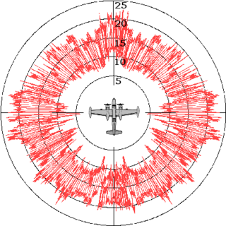
Radar cross-section (RCS), also called radar signature, is a measure of how detectable an object is by radar. A larger RCS indicates that an object is more easily detected.
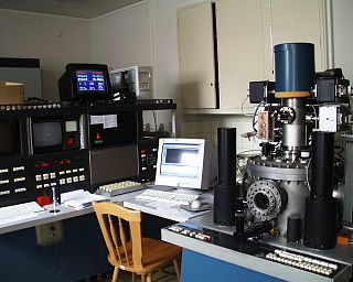
Electron-beam lithography is the practice of scanning a focused beam of electrons to draw custom shapes on a surface covered with an electron-sensitive film called a resist (exposing). The electron beam changes the solubility of the resist, enabling selective removal of either the exposed or non-exposed regions of the resist by immersing it in a solvent (developing). The purpose, as with photolithography, is to create very small structures in the resist that can subsequently be transferred to the substrate material, often by etching.
Masklesslithography (MPL) is a photomask-less photolithography-like technology used to project or focal-spot write the image pattern onto a chemical resist-coated substrate by means of UV radiation or electron beam.
Nanolithography (NL) is a growing field of techniques within nanotechnology dealing with the engineering of nanometer-scale structures on various materials.

Extreme ultraviolet lithography is an optical lithography technology used in steppers, machines that make integrated circuits (ICs) for computers and other electronic devices. It uses a range of extreme ultraviolet (EUV) wavelengths, roughly spanning a 2% FWHM bandwidth about 13.5 nm, to produce a pattern by exposing reflective photomask to UV light which gets reflected onto a substrate covered by photoresist. It is widely applied in semiconductor device fabrication process.
Next-generation lithography or NGL is a term used in integrated circuit manufacturing to describe the lithography technologies in development which are intended to replace current techniques. The term applies to any lithography method which uses a shorter-wavelength light or beam type than the current state of the art, such as X-ray lithography, electron beam lithography, focused ion beam lithography, and nanoimprint lithography. The term may also be used to describe techniques which achieve finer resolution features from an existing light wavelength.
Etec Systems was an American producer of scanning electron microscopes, electron beam lithography tools, and laser beam lithography tools from 1970 until 2005. It was located in Hayward, California, and Hillsboro, Oregon.
KLA Corporation is an American capital equipment company based in Milpitas, California. It supplies process control and yield management systems for the semiconductor industry and other related nanoelectronics industries. The company's products and services are intended for all phases of wafer, reticle, integrated circuit (IC) and packaging production, from research and development to final volume manufacturing.
Optical proximity correction (OPC) is a photolithography enhancement technique commonly used to compensate for image errors due to diffraction or process effects. The need for OPC is seen mainly in the making of semiconductor devices and is due to the limitations of light to maintain the edge placement integrity of the original design, after processing, into the etched image on the silicon wafer. These projected images appear with irregularities such as line widths that are narrower or wider than designed, these are amenable to compensation by changing the pattern on the photomask used for imaging. Other distortions such as rounded corners are driven by the resolution of the optical imaging tool and are harder to compensate for. Such distortions, if not corrected for, may significantly alter the electrical properties of what was being fabricated. Optical proximity correction corrects these errors by moving edges or adding extra polygons to the pattern written on the photomask. This may be driven by pre-computed look-up tables based on width and spacing between features or by using compact models to dynamically simulate the final pattern and thereby drive the movement of edges, typically broken into sections, to find the best solution,. The objective is to reproduce on the semiconductor wafer, as well as possible, the original layout drawn by the designer.
Resolution enhancement technologies are methods used to modify the photomasks in the lithographic processes used to make integrated circuits to compensate for limitations in the optical resolution of the projection systems. These processes allow the creation of features well beyond the limit that would normally apply due to the Rayleigh criterion. Modern technologies allow the creation of features on the order of 5 nanometers (nm), far below the normal resolution possible using deep ultraviolet (DUV) light.
Mask data preparation (MDP), also known as layout post processing, is the procedure of translating a file containing the intended set of polygons from an integrated circuit layout into set of instructions that a photomask writer can use to generate a physical mask. Typically, amendments and additions to the chip layout are performed in order to convert the physical layout into data for mask production.

LIGA is a fabrication technology used to create high-aspect-ratio microstructures. The term is a German acronym for Lithographie, Galvanoformung, Abformung – lithography, electroplating, and molding.
A mask shop is a factory which manufactures photomasks for use in the semiconductor industry. There are two distinct types found in the trade. Captive mask shops are in-house operations owned by the biggest semiconductor corporations, while merchant mask shops make masks for most of the industry.
Computational lithography is the set of mathematical and algorithmic approaches designed to improve the resolution attainable through photolithography. Computational lithography has come to the forefront of photolithography in 2008 as the semiconductor industry grappled with the challenges associated with the transition to 22 nanometer CMOS fabrication process technology and beyond.
Three-dimensional (3D) microfabrication refers to manufacturing techniques that involve the layering of materials to produce a three-dimensional structure at a microscopic scale. These structures are usually on the scale of micrometers and are popular in microelectronics and microelectromechanical systems.

JCMsuite is a finite element analysis software package for the simulation and analysis of electromagnetic waves, elasticity and heat conduction. It also allows a mutual coupling between its optical, heat conduction and continuum mechanics solvers. The software is mainly applied for the analysis and optimization of nanooptical and microoptical systems. Its applications in research and development projects include dimensional metrology systems, photolithographic systems, photonic crystal fibers, VCSELs, Quantum-Dot emitters, light trapping in solar cells, and plasmonic systems. The design tasks can be embedded into the high-level scripting languages MATLAB and Python, enabling a scripting of design setups in order to define parameter dependent problems or to run parameter scans.
