Katherine Jungjohann | |
|---|---|
| Education | Ph.D., Materials Science and Engineering |
| Alma mater | University of California, Davis |
| Occupation | Group Leader |
| Employer | National Renewable Energy Laboratory |
| Website | https://www.nrel.gov/research/staff/katherine-jungjohann.html |
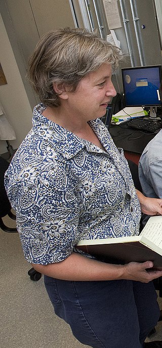
Katherine Jungjohann is a group leader at the National Renewable Energy Laboratory (NREL) [1] and previously worked as a scientist and engineer at the Center for Integrated Nanotechnologies (CINT) [2] [3] [4] which is part of Sandia National Laboratories [5] in Albuquerque, New Mexico, United States.
Jungjohann grew up in an academic family. [4]
Jungjohann received her Bachelor of Science degree in chemistry with honors from the University of Redlands, California, in 2008. She completed her Doctor of Philosophy degree in materials science and engineering at the University of California, Davis, CA in 2012. [6]
Jungjohann finished off a postdoctoral fellowship at the Center for Functional Nanomaterials at Brookhaven National Laboratory before beginning a staff position at the Center for Integrated Nanotechnologies at Sandia National Laboratories in 2013. [7] In 2021, Jungjohann joined the National Renewable Energy Laboratory (NREL) as a group manager.
Jungjohann has over 150 publications. Her most cited work has been cited over 300 times.
Here is a sampling of her most cited works, each one has been cited more than 100 times: [12]
JE Evans, KL Jungjohann, ND Browning, I Arslan (2011)
Y Liu, F Fan, J Wang, Y Liu, H Chen, KL Jungjohann, Y Xu, Y Zhu, D Bigio, ... (2014)
TJ Woehl, KL Jungjohann, JE Evans, I Arslan, WD Ristenpart, ... (2013)
KL Jungjohann, S Bliznakov, PW Sutter, EA Stach, EA Sutter (2013)
E Sutter, K Jungjohann, S Bliznakov, A Courty, E Maisonhaute, S Tenney, ... (2014)
KL Jungjohann, JE Evans, JA Aguiar, I Arslan, ND Browning (2012)
AJ Leenheer, KL Jungjohann, KR Zavadil, JP Sullivan, CT Harris (2015) [12]

Nanotechnology was defined by the National Nanotechnology Initiative as the manipulation of matter with at least one dimension sized from 1 to 100 nanometers (nm). At this scale, commonly known as the nanoscale, surface area and quantum mechanical effects become important in describing properties of matter. The definition of nanotechnology is inclusive of all types of research and technologies that deal with these special properties. It is therefore common to see the plural form "nanotechnologies" as well as "nanoscale technologies" to refer to the broad range of research and applications whose common trait is size. An earlier description of nanotechnology referred to the particular technological goal of precisely manipulating atoms and molecules for fabrication of macroscale products, also now referred to as molecular nanotechnology.

Transmission electron microscopy (TEM) is a microscopy technique in which a beam of electrons is transmitted through a specimen to form an image. The specimen is most often an ultrathin section less than 100 nm thick or a suspension on a grid. An image is formed from the interaction of the electrons with the sample as the beam is transmitted through the specimen. The image is then magnified and focused onto an imaging device, such as a fluorescent screen, a layer of photographic film, or a sensor such as a scintillator attached to a charge-coupled device.

Nanomaterials describe, in principle, materials of which a single unit is sized between 1 and 100 nm.

A scanning transmission electron microscope (STEM) is a type of transmission electron microscope (TEM). Pronunciation is [stɛm] or [ɛsti:i:ɛm]. As with a conventional transmission electron microscope (CTEM), images are formed by electrons passing through a sufficiently thin specimen. However, unlike CTEM, in STEM the electron beam is focused to a fine spot which is then scanned over the sample in a raster illumination system constructed so that the sample is illuminated at each point with the beam parallel to the optical axis. The rastering of the beam across the sample makes STEM suitable for analytical techniques such as Z-contrast annular dark-field imaging, and spectroscopic mapping by energy dispersive X-ray (EDX) spectroscopy, or electron energy loss spectroscopy (EELS). These signals can be obtained simultaneously, allowing direct correlation of images and spectroscopic data.

Nanometrology is a subfield of metrology, concerned with the science of measurement at the nanoscale level. Nanometrology has a crucial role in order to produce nanomaterials and devices with a high degree of accuracy and reliability in nanomanufacturing.
The following outline is provided as an overview of and topical guide to nanotechnology:

Nestor J. Zaluzec is an American scientist and inventor who works at Argonne National Laboratory. He invented and patented the Scanning Confocal Electron Microscope. and the π Steradian Transmission X-ray Detector for Electron-Optical Beam Lines and Microscopes.

The National Synchrotron Light Source II (NSLS-II) at Brookhaven National Laboratory (BNL) in Upton, New York is a national user research facility funded primarily by the U.S. Department of Energy's (DOE) Office of Science. NSLS-II is one of the world's most advanced synchrotron light sources, designed to produce x-rays 10,000 times brighter than BNL's original light source, the National Synchrotron Light Source (NSLS). NSLS-II supports basic and applied research in energy security, advanced materials synthesis and manufacturing, environment, and human health.
MEMS for in situ mechanical characterization refers to microelectromechanical systems (MEMS) used to measure the mechanical properties of nanoscale specimens such as nanowires, nanorods, whiskers, nanotubes and thin films. They distinguish themselves from other methods of nanomechanical testing because the sensing and actuation mechanisms are embedded and/or co-fabricated in the microsystem, providing—in the majority of cases—greater sensitivity and precision.
C. Barry Carter is a professor of Materials Science and Engineering at the University of Connecticut in Storrs, Connecticut. He is a CINT Distinguished Affiliate Scientist at Sandia National Laboratories and editor-in-chief of the Journal of Materials Science. Carter's research areas of focus include Transmission Electron Microscopy and Atomic-force microscopy.
In situ electron microscopy is an investigatory technique where an electron microscope is used to watch a sample's response to a stimulus in real time. Due to the nature of the high-energy beam of electrons used to image a sample in an electron microscope, microscopists have long observed that specimens are routinely changed or damaged by the electron beam. Starting in the 1960s, and using transmission electron microscopes (TEMs), scientists made deliberate attempts to modify materials while the sample was in the specimen chamber, and to capture images through time of the induced damages.

Alexander V. Balatsky is a USSR-born American physicist. He is the professor of theoretical physics at NORDITA and University of Connecticut. He served as the founding director of the Institute for Materials Science (IMS) at Los Alamos National Laboratory in 2014–2017.
The health and safety hazards of nanomaterials include the potential toxicity of various types of nanomaterials, as well as fire and dust explosion hazards. Because nanotechnology is a recent development, the health and safety effects of exposures to nanomaterials, and what levels of exposure may be acceptable, are subjects of ongoing research. Of the possible hazards, inhalation exposure appears to present the most concern, with animal studies showing pulmonary effects such as inflammation, fibrosis, and carcinogenicity for some nanomaterials. Skin contact and ingestion exposure, and dust explosion hazards, are also a concern.

Liquid-phase electron microscopy refers to a class of methods for imaging specimens in liquid with nanometer spatial resolution using electron microscopy. LP-EM overcomes the key limitation of electron microscopy: since the electron optics requires a high vacuum, the sample must be stable in a vacuum environment. Many types of specimens relevant to biology, materials science, chemistry, geology, and physics, however, change their properties when placed in a vacuum.

The characterization of nanoparticles is a branch of nanometrology that deals with the characterization, or measurement, of the physical and chemical properties of nanoparticles. Nanoparticles measure less than 100 nanometers in at least one of their external dimensions, and are often engineered for their unique properties. Nanoparticles are unlike conventional chemicals in that their chemical composition and concentration are not sufficient metrics for a complete description, because they vary in other physical properties such as size, shape, surface properties, crystallinity, and dispersion state.

Titanium dioxide nanoparticles, also called ultrafine titanium dioxide or nanocrystalline titanium dioxide or microcrystalline titanium dioxide, are particles of titanium dioxide with diameters less than 100 nm. Ultrafine TiO2 is used in sunscreens due to its ability to block ultraviolet radiation while remaining transparent on the skin. It is in rutile crystal structure and coated with silica or/and alumina to prevent photocatalytic phenomena. The health risks of ultrafine TiO2 from dermal exposure on intact skin are considered extremely low, and it is considered safer than other substances used for ultraviolet protection.

Frances Mary Ross is the Ellen Swallow Richards Professor in Materials Science and Engineering at Massachusetts Institute of Technology. Her work involves the use of in situ transmission electron microscopy to study nanostructure formation. In 2018 she was awarded the International Federation of Societies for Microscopy Hatsujiro Hashimoto Medal. Ross is a Fellow of the American Association for the Advancement of Science, the American Physical Society, the Microscopy Society of America and the Royal Microscopical Society,
The National User Facilities are a set of large-scale scientific facilities maintained by the U.S. Department of Energy, Office of Science, whose roles are to provide the scientific community with world-leading scientific instruments to enable research. These facilities are generally free to use, and are open to scientists from all over the world, usually through the submission and evaluation of research proposals.

The "Centre d’Élaboration de Matériaux et d’Etudes Structurales" (CEMES) is a CNRS laboratory located in Toulouse, France.

Ilke Arslan is a Turkish American microscopist who is Director of the Center for Nanoscale Materials and the Nanoscience and Technology division at Argonne National Laboratory. She was awarded the Presidential Early Career Award for Scientists and Engineers in 2010 and appointed to the Oppenheimer Science and Energy Leadership Program in 2020.