Related Research Articles

Germanium is a chemical element; it has symbol Ge and atomic number 32. It is lustrous, hard-brittle, grayish-white and similar in appearance to silicon. It is a metalloid in the carbon group that is chemically similar to its group neighbors silicon and tin. Like silicon, germanium naturally reacts and forms complexes with oxygen in nature.
A nanowire is a nanostructure in the form of a wire with the diameter of the order of a nanometre. More generally, nanowires can be defined as structures that have a thickness or diameter constrained to tens of nanometers or less and an unconstrained length. At these scales, quantum mechanical effects are important—which coined the term "quantum wires".
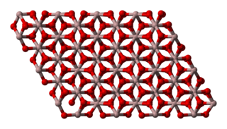
Aluminium oxide (or aluminium(III) oxide) is a chemical compound of aluminium and oxygen with the chemical formula Al2O3. It is the most commonly occurring of several aluminium oxides, and specifically identified as aluminium oxide. It is commonly called alumina and may also be called aloxide, aloxite, or alundum in various forms and applications. It occurs naturally in its crystalline polymorphic phase α-Al2O3 as the mineral corundum, varieties of which form the precious gemstones ruby and sapphire. Al2O3 is significant in its use to produce aluminium metal, as an abrasive owing to its hardness, and as a refractory material owing to its high melting point.

A photonic crystal is an optical nanostructure in which the refractive index changes periodically. This affects the propagation of light in the same way that the structure of natural crystals gives rise to X-ray diffraction and that the atomic lattices of semiconductors affect their conductivity of electrons. Photonic crystals occur in nature in the form of structural coloration and animal reflectors, and, as artificially produced, promise to be useful in a range of applications.

Sandpaper, also known as glasspaper or as coated abrasive, is a type of material that consists of sheets of paper or cloth with an abrasive substance glued to one face. In the modern manufacture of these products, sand and glass have been replaced by other abrasives such as aluminium oxide or silicon carbide. It is common to use the name of the abrasive when describing the paper, e.g. "aluminium oxide paper", or "silicon carbide paper".

The vertical-cavity surface-emitting laser is a type of semiconductor laser diode with laser beam emission perpendicular from the top surface, contrary to conventional edge-emitting semiconductor lasers which emit from surfaces formed by cleaving the individual chip out of a wafer. VCSELs are used in various laser products, including computer mice, fiber optic communications, laser printers, Face ID, and smartglasses.
Liquid crystal on silicon is a miniaturized reflective active-matrix liquid-crystal display or "microdisplay" using a liquid crystal layer on top of a silicon backplane. It is also known as a spatial light modulator. LCoS initially was developed for projection televisions, but has since found additional uses in wavelength selective switching, structured illumination, near-eye displays and optical pulse shaping.

An optical fiber, or optical fibre, is a flexible glass or plastic fiber that can transmit light from one end to the other. Such fibers find wide usage in fiber-optic communications, where they permit transmission over longer distances and at higher bandwidths than electrical cables. Fibers are used instead of metal wires because signals travel along them with less loss and are immune to electromagnetic interference. Fibers are also used for illumination and imaging, and are often wrapped in bundles so they may be used to carry light into, or images out of confined spaces, as in the case of a fiberscope. Specially designed fibers are also used for a variety of other applications, such as fiber optic sensors and fiber lasers.
A hydrogen sensor is a gas detector that detects the presence of hydrogen. They contain micro-fabricated point-contact hydrogen sensors and are used to locate hydrogen leaks. They are considered low-cost, compact, durable, and easy to maintain as compared to conventional gas detecting instruments.
A photonic integrated circuit (PIC) or integrated optical circuit is a microchip containing two or more photonic components that form a functioning circuit. This technology detects, generates, transports, and processes light. Photonic integrated circuits utilize photons as opposed to electrons that are utilized by electronic integrated circuits. The major difference between the two is that a photonic integrated circuit provides functions for information signals imposed on optical wavelengths typically in the visible spectrum or near infrared (850–1650 nm).

Silicon photonics is the study and application of photonic systems which use silicon as an optical medium. The silicon is usually patterned with sub-micrometre precision, into microphotonic components. These operate in the infrared, most commonly at the 1.55 micrometre wavelength used by most fiber optic telecommunication systems. The silicon typically lies on top of a layer of silica in what is known as silicon on insulator (SOI).

Fiber-optic communication is a method of transmitting information from one place to another by sending pulses of infrared or visible light through an optical fiber. The light is a form of carrier wave that is modulated to carry information. Fiber is preferred over electrical cabling when high bandwidth, long distance, or immunity to electromagnetic interference is required. This type of communication can transmit voice, video, and telemetry through local area networks or across long distances.
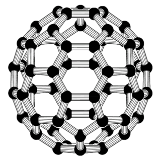
Carbon nanotubes (CNTs) are cylinders of one or more layers of graphene (lattice). Diameters of single-walled carbon nanotubes (SWNTs) and multi-walled carbon nanotubes (MWNTs) are typically 0.8 to 2 nm and 5 to 20 nm, respectively, although MWNT diameters can exceed 100 nm. CNT lengths range from less than 100 nm to 0.5 m.

A slot-waveguide is an optical waveguide that guides strongly confined light in a subwavelength-scale low refractive index region by total internal reflection.
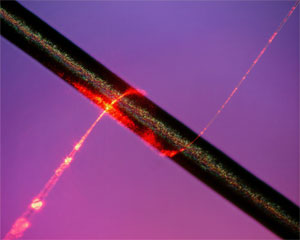
A subwavelength-diameter optical fibre is an optical fibre whose diameter is less than the wavelength of the light being propagated through it. An SDF usually consists of long thick parts at both ends, transition regions (tapers) where the fibre diameter gradually decreases down to the subwavelength value, and a subwavelength-diameter waist, which is the main acting part. Due to such a strong geometrical confinement, the guided electromagnetic field in an SDF is restricted to a single mode called fundamental.
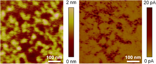
In microscopy, conductive atomic force microscopy (C-AFM) or current sensing atomic force microscopy (CS-AFM) is a mode in atomic force microscopy (AFM) that simultaneously measures the topography of a material and the electric current flow at the contact point of the tip with the surface of the sample. The topography is measured by detecting the deflection of the cantilever using an optical system, while the current is detected using a current-to-voltage preamplifier. The fact that the CAFM uses two different detection systems is a strong advantage compared to scanning tunneling microscopy (STM). Basically, in STM the topography picture is constructed based on the current flowing between the tip and the sample. Therefore, when a portion of a sample is scanned with an STM, it is not possible to discern if the current fluctuations are related to a change in the topography or to a change in the sample conductivity.
The technique of vibrational analysis with scanning probe microscopy allows probing vibrational properties of materials at the submicrometer scale, and even of individual molecules. This is accomplished by integrating scanning probe microscopy (SPM) and vibrational spectroscopy. This combination allows for much higher spatial resolution than can be achieved with conventional Raman/FTIR instrumentation. The technique is also nondestructive, requires non-extensive sample preparation, and provides more contrast such as intensity contrast, polarization contrast and wavelength contrast, as well as providing specific chemical information and topography images simultaneously.

Orbital angular momentum (OAM) multiplexing is a physical layer method for multiplexing signals carried on electromagnetic waves using the orbital angular momentum of the electromagnetic waves to distinguish between the different orthogonal signals.

Alexander Coucoulas is an American inventor, research engineer, and author. He was named "father of thermosonic bonding" by George Harman, the world's foremost authority on wire bonding, where he referenced Coucoulas's leading edge publications in his book, Wire Bonding In Microelectronics. A thermosonic bond is formed using a set of parameters which include ultrasonic, thermal and mechanical (force) energies.

Prof. R K Sinha is the Vice Chancellor of Gautam Buddha University, Greater Noida, Gautam Budh Nagar Under UP Government. He was the director of the CSIR-Central Scientific Instruments Organisation (CSIR-CSIO) Sector-30C, Chandigarh-160 030, India. He has been a Professor - Applied Physics, Dean-Academic [UG] & Chief Coordinator: TIFAC-Center of Relevance and Excellence in Fiber Optics and Optical Communication, Mission REACH Program, Technology Vision-2020, Govt. of India Delhi Technological University Bawana Road, Delhi-110042, India.
References
- ↑ Şimşek, E.U.; Şimşek, B.; Ortaç, B. (2017). "CO 2 laser polishing of conical shaped optical fiber deflectors". Applied Physics B . 123 (6): 1–9. doi:10.1007/s00340-017-6746-3. hdl: 11693/36371 . S2CID 46932150.
- ↑ Saleem Hashmi (2016). Comprehensive Materials Finishing. Vol. 1–3. Elsevier Science. p. 102. ISBN 9780128032503.
- 1 2 Davenport, John J.; Hickey, Michelle; Phillips, Justin P.; Kyriacou, Panayiotis (2016). "Method for producing angled optical fiber tips in the laboratory" (PDF). Optical Engineering . 55 (2): 026120. Bibcode:2016OptEn..55b6120D. doi:10.1117/1.OE.55.2.026120. S2CID 32806740.
- ↑ Dobb, H.; Carroll, K.; Webb, D.J.; Kalli, K.; Komodromos, M.; Themistos, C.; Peng, G.D.; Argyros, A.; Large, M.C.J.; Van Eijkelenborg, M.A.; Arresy, M. (2006). Limberger, Hans G.; Matthewson, M. John (eds.). "Reliability of fibre Bragg gratings in polymer optical fibre" (PDF). Reliability of Optical Fiber Components, Devices, Systems, and Networks III. 6193. SPIE: 203–214. Bibcode:2006SPIE.6193E..0QD. doi:10.1117/12.662313. S2CID 54175894.
- ↑ Zheng, L.B.; Xie, J.; Na, T.K.; Xie, H.F. (2012). "Micro Grinding Technique of Mutilcore Fiber Endface Using 3D Flock-structured Film". Advanced Materials Research. 426: 243–246. doi:10.4028/www.scientific.net/AMR.426.243. S2CID 135749447.