
The technology of computer keyboards includes many elements. Many different keyboard technologies have been developed for consumer demands and optimized for industrial applications. The standard full-size (100%) computer alphanumeric keyboard typically uses 101 to 105 keys; keyboards integrated in laptop computers are typically less comprehensive.

Organic electronics is a field of materials science concerning the design, synthesis, characterization, and application of organic molecules or polymers that show desirable electronic properties such as conductivity. Unlike conventional inorganic conductors and semiconductors, organic electronic materials are constructed from organic (carbon-based) molecules or polymers using synthetic strategies developed in the context of organic chemistry and polymer chemistry.

In electrical engineering, a switch is an electrical component that can disconnect or connect the conducting path in an electrical circuit, interrupting the electric current or diverting it from one conductor to another. The most common type of switch is an electromechanical device consisting of one or more sets of movable electrical contacts connected to external circuits. When a pair of contacts is touching current can pass between them, while when the contacts are separated no current can flow.

Electromagnetic compatibility (EMC) is the ability of electrical equipment and systems to function acceptably in their electromagnetic environment, by limiting the unintentional generation, propagation and reception of electromagnetic energy which may cause unwanted effects such as electromagnetic interference (EMI) or even physical damage to operational equipment. The goal of EMC is the correct operation of different equipment in a common electromagnetic environment. It is also the name given to the associated branch of electrical engineering.

In electrical engineering, ground or earth may be a reference point in an electrical circuit from which voltages are measured, a common return path for electric current, or a direct physical connection to the Earth.

A printed circuit board (PCB), also called printed wiring board (PWB), is a medium used to connect or "wire" components to one another in a circuit. It takes the form of a laminated sandwich structure of conductive and insulating layers: each of the conductive layers is designed with a pattern of traces, planes and other features etched from one or more sheet layers of copper laminated onto and/or between sheet layers of a non-conductive substrate. Electrical components may be fixed to conductive pads on the outer layers in the shape designed to accept the component's terminals, generally by means of soldering, to both electrically connect and mechanically fasten them to it. Another manufacturing process adds vias, plated-through holes that allow interconnections between layers.

Flexible electronics, also known as flex circuits, is a technology for assembling electronic circuits by mounting electronic devices on flexible plastic substrates, such as polyimide, PEEK or transparent conductive polyester film. Additionally, flex circuits can be screen printed silver circuits on polyester. Flexible electronic assemblies may be manufactured using identical components used for rigid printed circuit boards, allowing the board to conform to a desired shape, or to flex during its use.
Indium tin oxide (ITO) is a ternary composition of indium, tin and oxygen in varying proportions. Depending on the oxygen content, it can be described as either a ceramic or an alloy. Indium tin oxide is typically encountered as an oxygen-saturated composition with a formulation of 74% In, 8% Sn, and 18% O by weight. Oxygen-saturated compositions are so typical that unsaturated compositions are termed oxygen-deficient ITO. It is transparent and colorless in thin layers, while in bulk form it is yellowish to gray. In the infrared region of the spectrum it acts as a metal-like mirror.

A membrane keyboard is a computer keyboard whose "keys" are not separate, moving parts, as with the majority of other keyboards, but rather are pressure pads that have only outlines and symbols printed on a flat, flexible surface. Very little, if any, tactile feedback is felt when using such a keyboard.
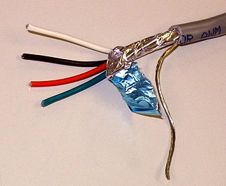
A shielded cable or screened cable is an electrical cable that has a common conductive layer around its conductors for electromagnetic shielding. This shield is usually covered by an outermost layer of the cable. Common types of cable shielding can most broadly be categorized as foil type, contraspiralling wire strands or both. A longitudinal wire may be necessary with dielectric spiral foils to short out each turn.
Conductive ink is an ink that results in a printed object which conducts electricity. It is typically created by infusing graphite or other conductive materials into ink. There has been a growing interest in replacing metallic materials with nanomaterials due to the emergence of nanotechnology. Among other nanomaterials, graphene, and carbon nanotube-based conductive ink are gaining immense popularity due to their high electrical conductivity and high surface area. Recently, more attention has been paid on using eco-friendly conductive ink using water as a solvent as compared to organic solvents since they are harmful to the environment. However, the high surface tension of water prevents its applicability. Various natural and synthetic surfactants are now used to reduce the surface tension of water and ensure uniform nanomaterials dispersibility for smooth printing and wide application. Although graphene oxide inks are eco-friendly and can be produced in bulk quantities, they are insulating in nature which needs an additional step of reduction using reducing ink is required to restore the electrical properties. The external reduction process is not suitable for large scale continuous manufacturing of electronic devices. Hence an in-situ reduction process also known as reactive inkjet printing has been developed by various scientists. In the in-situ reduction process the reducing inks are printed on top of the GO printed patterns in order to carry out the reduction process on the substrate.

Printed electronics is a set of printing methods used to create electrical devices on various substrates. Printing typically uses common printing equipment suitable for defining patterns on material, such as screen printing, flexography, gravure, offset lithography, and inkjet. By electronic-industry standards, these are low-cost processes. Electrically functional electronic or optical inks are deposited on the substrate, creating active or passive devices, such as thin film transistors; capacitors; coils; resistors. Some researchers expect printed electronics to facilitate widespread, very low-cost, low-performance electronics for applications such as flexible displays, smart labels, decorative and animated posters, and active clothing that do not require high performance.

A conductive textile is a fabric which can conduct electricity. Conductive textiles known as lamé are made with guipé thread or yarn that is conductive because it is composed of metallic fibers wrapped around a non-metallic core or has a metallic coating. A different way of achieving conductivity is to weave metallic strands into the textile.
Silicone rubber keypads are used extensively in both consumer and industrial electronic products as a low cost and reliable switching solution.
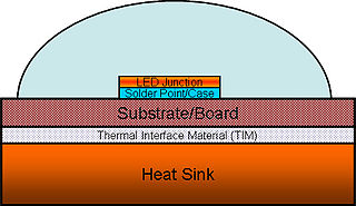
High power light-emitting diodes (LEDs) can use 350 milliwatts or more in a single LED. Most of the electricity in an LED becomes heat rather than light. If this heat is not removed, the LEDs run at high temperatures, which not only lowers their efficiency, but also makes the LED less reliable. Thus, thermal management of high power LEDs is a crucial area of research and development. It is necessary to limit both the junction and the phosphor particles temperatures to a value that will guarantee the desired LED lifetime.
Photonic curing is the high-temperature thermal processing of a thin film using pulsed light from a flashlamp. When this transient processing is done on a low-temperature substrate such as plastic or paper, it is possible to attain a significantly higher temperature than the substrate can ordinarily withstand under an equilibrium heating source such as an oven. Since the rate of most thermal curing processes generally increase exponentially with temperature, this process allows materials to be cured much more rapidly than with an oven.
An electrically conductive adhesive is a glue that is primarily used for electronics.
Circuit Scribe is a ball-point pen containing silver conductive ink one can use to draw circuits instantly on flexible substrates like paper. Circuit Scribe made its way onto Kickstarter on November 19, 2013, with its goal of raising $85,000 for the manufacturing of the first batch of pens. By December 31, 2013, Circuit Scribe was able to raise a total of $674,425 with 12,277 'backers' or donors.

Chip on board (COB) is a method of circuit board manufacturing in which the integrated circuits (e.g. microprocessors) are attached (wired, bonded directly) to a printed circuit board, and covered by a blob of epoxy. Chip on board eliminates the packaging of individual semiconductor devices, which allows a completed product to be less costly, lighter, and more compact. In some cases, COB construction improves the operation of radio frequency systems by reducing the inductance and capacitance of integrated circuit leads.

Copper foil is a thin sheet of copper metal that is widely used in various applications due to its excellent electrical conductivity, malleability, and corrosion resistance. It is an essential material in the electronics industry, especially for manufacturing printed circuit boards (PCBs) and other electronic components.
