Microvia

Last updated

Microvias are used as the interconnects between layers in high density interconnect (HDI) substrates and printed circuit boards (PCBs) to accommodate the high input/output (I/O) density of advanced packages. Driven by portability and wireless communications, the electronics industry strives to produce affordable, light, and reliable products with increased functionality. At the electronic component level, this translates to components with increased I/Os with smaller footprint areas (e.g. flip-chip packages, chip-scale packages, and direct chip attachments), and on the printed circuit board and package substrate level, to the use of high density interconnects (HDIs) (e.g. finer lines and spaces, and smaller vias). [1]

Contents

Overview

IPC standards revised the definition of a microvia in 2013 to a hole with depth to diameter aspect ratio of 1:1 or less, and the hole depth not to exceed 0.25mm. Previously, microvia was any hole less than or equal to 0.15mm in diameter [2]

With the advent of smartphones and hand-held electronic devices, microvias have evolved from single-level to stacked microvias that cross over multiple HDI layers. Sequential build-up (SBU) technology is used to fabricate HDI boards. The HDI layers are usually built up from a traditionally manufactured double-sided core board or multilayer PCB. The HDI layers are built on both sides of the traditional PCB one by one with microvias. The SBU process consists of several steps: layer lamination, via formation, via metallization, and via filling. There are multiple choices of materials and/or technologies for each step. [3]

Microvias can be filled with different materials and processes: [4]

  1. Filled with epoxy resin (b-stage) during a sequential lamination process step
  2. Filled with non-conductive or conductive material other than copper as a separate processing step
  3. Plated closed with electroplated copper
  4. Screen printed closed with a copper paste

Buried microvias are required to be filled, while blind microvias on the external layers usually do not have any fill requirements. [5] A stacked microvia is usually filled with electroplated copper to make electrical interconnections between multiple HDI layers and provide structural support for the outer level(s) of the microvia or for a component mounted on the outermost copper pad. [6] [7]

Microvia reliability

The reliability of HDI structure is one of the major constraints for its successful widespread implementation in the PCB industry. Good thermo-mechanical reliability of microvias is an essential part of HDI reliability. Many researchers and professionals have studied the reliability of microvias in HDI PCBs. The reliability of microvias depends on many factors such as microvia geometry parameters, dielectric material properties, and processing parameters.

Microvia reliability research has focused on experimental assessment of the reliability of single-level unfilled microvias, as well as finite element analysis on stress/strain distributions in single-level microvias and microvia fatigue life estimation. [8] Microvia failures identified from the research include interfacial separation (separation between the base of the microvia and the target pad), barrel cracks, corner/knee cracks, and target pad cracks (also referred to as microvia pull out). These failures result from the thermomechanical stresses caused by coefficient of thermal expansion (CTE) mismatch, in the PCB thickness direction, between the metallization in a microvia structure and the dielectric materials surrounding the metal. The following paragraph highlights some of the microvia reliability research.

Ogunjimi et al. [9] looked at the effect of manufacturing and design process variables on the fatigue life of microvias, including trace (conductor) thickness, layer or layers of the dielectric around the trace and in the microvia, via geometry, via wall angle, ductility coefficient of the conductor material, and strain concentration factor. Finite element models were created with different geometries, and ANOVA method was used to determine the significance of the different process variables. The ANOVA results showed that the strain concentration factor was the most important variable, followed with the ductility factor, metallization thickness, and via wall angle. Prabhu et al. [10] conducted a finite element analysis (FEA) on an HDI microvia structure to determine the effect of accelerated temperature cycling and thermal shock. Liu et al. [11] and Ramakrishna et al. [12] conducted liquid-to-liquid and air-to-air thermal shock testing, respectively, to studied the effect of dielectric material properties and microvia geometry parameters, such as microvia diameter, wall angle and plating thickness, on microvia reliability. Andrews et al. [13] investigated single-level microvia reliability using IST (interconnect stress test), and considered the effect of reflow cycles of lead-free solder. Wang and Lai [14] investigated the potential failure sites of microvias using finite element modeling. They found that filled microvias have a lower stress than unfilled microvias. Choi and Dasgupta introduced microvia non-destructive inspection method in their work. [15]

Although most microvia reliability research focuses on single-level microvias, Birch [4] tested multiple-level stacked and staggered microvias using IST test. Weibull analysis on the test data showed that single- and 2-level stacked microvias last longer than 3- and 4-level microvias (e. g. 2-level stacked microvias experienced about 20 times more cycles to failure than 4-level stacked microvias).

a cross-section view of a microvia with a void MicroviaVoiding.png
a cross-section view of a microvia with a void

Microvia voiding

One challenge for high density interconnect board development, is to fabricate reliable microvias, especially for stacked microvias, without resulting in incomplete filling, dimples, or voids in the copper plating process. [16] The authors of [16] have been investigating the risk of microvias in terms of voids and other defects using both experimental testing and finite element analysis. They found that incomplete copper filling increases the stress levels in microvias and hence decreases microvia fatigue life.

As for voids, different voiding conditions, such as different void sizes, shapes, and locations result in different effects on microvia reliability. Small voids of a spherical shape lightly increase the microvia fatigue life, but extreme voiding conditions greatly reduce the duration of microvias.

Related Research Articles

<span class="mw-page-title-main">Printed circuit board</span> Board to support and connect electronic components

A printed circuit board (PCB), also called printed wiring board (PWB), is a medium used to connect or "wire" components to one another in a circuit. It takes the form of a laminated sandwich structure of conductive and insulating layers: each of the conductive layers is designed with a pattern of traces, planes and other features etched from one or more sheet layers of copper laminated onto and/or between sheet layers of a non-conductive substrate. Electrical components may be fixed to conductive pads on the outer layers in the shape designed to accept the component's terminals, generally by means of soldering, to both electrically connect and mechanically fasten them to it. Another manufacturing process adds vias, plated-through holes that allow interconnections between layers.

<span class="mw-page-title-main">Wire bonding</span> Technique used to connect a microchip to its package

Wire bonding is the method of making interconnections between an integrated circuit (IC) or other semiconductor device and its packaging during semiconductor device fabrication. Although less common, wire bonding can be used to connect an IC to other electronics or to connect from one printed circuit board (PCB) to another. Wire bonding is generally considered the most cost-effective and flexible interconnect technology and is used to assemble the vast majority of semiconductor packages. Wire bonding can be used at frequencies above 100 GHz.

In semiconductor technology, copper interconnects are interconnects made of copper. They are used in silicon integrated circuits (ICs) to reduce propagation delays and power consumption. Since copper is a better conductor than aluminium, ICs using copper for their interconnects can have interconnects with narrower dimensions, and use less energy to pass electricity through them. Together, these effects lead to ICs with better performance. They were first introduced by IBM, with assistance from Motorola, in 1997.

<span class="mw-page-title-main">Flexible electronics</span> Mounting of electronic devices on flexible plastic substrates

Flexible electronics, also known as flex circuits, is a technology for assembling electronic circuits by mounting electronic devices on flexible plastic substrates, such as polyimide, PEEK or transparent conductive polyester film. Additionally, flex circuits can be screen printed silver circuits on polyester. Flexible electronic assemblies may be manufactured using identical components used for rigid printed circuit boards, allowing the board to conform to a desired shape, or to flex during its use.

A via is an electrical connection between two or more metal layers, and are commonly used in printed circuit boards (PCB). Essentially a via is a small drilled hole that goes through two or more adjacent layers; the hole is plated with metal that forms an electrical connection through the insulating layers.

<span class="mw-page-title-main">Back end of line</span> Part of manufacturing process used to create integrated circuits

The back end of line (BEOL) is the second portion of IC fabrication where the individual devices get interconnected with wiring on the wafer, the metalization layer. Common metals are copper and aluminum. BEOL generally begins when the first layer of metal is deposited on the wafer. BEOL includes contacts, insulating layers (dielectrics), metal levels, and bonding sites for chip-to-package connections.

Conformal coating is a protective, breathable coating of thin polymeric film applied to printed circuit boards (PCBs). Conformal coatings are typically applied at 25–250 μm to the electronic circuitry and provide protection against moisture and other harsher conditions.

<span class="mw-page-title-main">Flat no-leads package</span> Integrated circuit package with contacts on all 4 sides, on the underside of the package

Flat no-leads packages such as quad-flat no-leads (QFN) and dual-flat no-leads (DFN) physically and electrically connect integrated circuits to printed circuit boards. Flat no-leads, also known as micro leadframe (MLF) and SON, is a surface-mount technology, one of several package technologies that connect ICs to the surfaces of PCBs without through-holes. Flat no-lead is a near chip scale plastic encapsulated package made with a planar copper lead frame substrate. Perimeter lands on the package bottom provide electrical connections to the PCB. Flat no-lead packages usually, but not always, include an exposed thermally conductive pad to improve heat transfer out of the IC. Heat transfer can be further facilitated by metal vias in the thermal pad. The QFN package is similar to the quad-flat package (QFP), and a ball grid array (BGA).

<span class="mw-page-title-main">IPC (electronics)</span> Trade association for electronics

IPC is a trade association whose aim is to standardize the assembly and production requirements of electronic equipment and assemblies. IPC is headquartered in Bannockburn, Illinois, United States with additional offices in Washington, D.C. Atlanta, Ga., and Miami, Fla. in the United States, and overseas offices in China, Japan, Thailand, India, Germany, and Belgium.

<span class="mw-page-title-main">Bead probe technology</span> Technique used for in-circuit testing

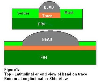
Bead probe technology (BPT) is technique used to provide electrical access to printed circuit board (PCB) circuitry for performing in-circuit testing (ICT). It makes use of small beads of solder placed onto the board's traces to allow measuring and controlling of the signals using a test probe. This permits test access to boards on which standard ICT test pads are not feasible due to space constraints.

<span class="mw-page-title-main">Thermal copper pillar bump</span>

The thermal copper pillar bump, also known as the "thermal bump", is a thermoelectric device made from thin-film thermoelectric material embedded in flip chip interconnects for use in electronics and optoelectronic packaging, including: flip chip packaging of CPU and GPU integrated circuits (chips), laser diodes, and semiconductor optical amplifiers (SOA). Unlike conventional solder bumps that provide an electrical path and a mechanical connection to the package, thermal bumps act as solid-state heat pumps and add thermal management functionality locally on the surface of a chip or to another electrical component. The diameter of a thermal bump is 238 μm and 60 μm high.

<span class="mw-page-title-main">Failure of electronic components</span> Ways electronic components fail and prevention measures

Electronic components have a wide range of failure modes. These can be classified in various ways, such as by time or cause. Failures can be caused by excess temperature, excess current or voltage, ionizing radiation, mechanical shock, stress or impact, and many other causes. In semiconductor devices, problems in the device package may cause failures due to contamination, mechanical stress of the device, or open or short circuits.

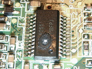
Pad cratering is a mechanically induced fracture in the resin between copper foil and outermost layer of fiberglass of a printed circuit board (PCB). It may be within the resin or at the resin to fiberglass interface.

Physics of failure is a technique under the practice of reliability design that leverages the knowledge and understanding of the processes and mechanisms that induce failure to predict reliability and improve product performance.

Solder fatigue is the mechanical degradation of solder due to deformation under cyclic loading. This can often occur at stress levels below the yield stress of solder as a result of repeated temperature fluctuations, mechanical vibrations, or mechanical loads. Techniques to evaluate solder fatigue behavior include finite element analysis and semi-analytical closed-form equations.

Digital image correlation analyses have applications in material property characterization, displacement measurement, and strain mapping. As such, DIC is becoming an increasingly popular tool when evaluating the thermo-mechanical behavior of electronic components and systems.

In electronics, a cross section, cross-section, or microsection, is a prepared electronics sample that allows analysis at a plane that cuts through the sample. It is a destructive technique requiring that a portion of the sample be cut or ground away to expose the internal plane for analysis. They are commonly prepared for research, manufacturing quality assurance, supplier conformity, and failure analysis. Printed wiring boards (PWBs) and electronic components and their solder joints are common cross sectioned samples. The features of interest to be analyzed in cross section can be nanometer-scale metal and dielectric layers in semiconductors up to macroscopic features such as the amount of solder that has filled into a large, 0.125in (3.18mm) diameter plated through hole.

Conductive anodic filament, also called CAF, is a metallic filament that forms from an electrochemical migration process and is known to cause printed circuit board (PCB) failures.

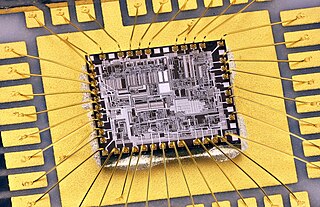
In integrated circuits (ICs), interconnects are structures that connect two or more circuit elements together electrically. The design and layout of interconnects on an IC is vital to its proper function, performance, power efficiency, reliability, and fabrication yield. The material interconnects are made from depends on many factors. Chemical and mechanical compatibility with the semiconductor substrate and the dielectric between the levels of interconnect is necessary, otherwise barrier layers are needed. Suitability for fabrication is also required; some chemistries and processes prevent the integration of materials and unit processes into a larger technology (recipe) for IC fabrication. In fabrication, interconnects are formed during the back-end-of-line after the fabrication of the transistors on the substrate.

Glossary of microelectronics manufacturing terms

References

  1. "Everything You Need to Know About Microvias in Printed Circuit Design". Altium. 2017-05-23. Retrieved 2022-09-29.
  2. https://blog.ipc.org/2014/01/10/new-microvia-definition-seeing-broader-usage/
  3. Happy Holden et al., The HDI Handbook, 1st Edition. Available from: http://www.hdihandbook.com/
  4. 1 2 B. Birch, “Reliability Testing for Microvias in Printed Wire Boards”, Circuit World, Vol. 35, No. 4, pp. 3 – 17, 2009
  5. IPC-6016, “Qualification and Performance Specification for High-density Interconnect (HDI) Structures,” May 1999
  6. "Microvia HDI PCB :All The Guidance You Need To Make The Right Choice". www.hemeixinpcb.com. Retrieved 2022-09-29.
  7. Forbus, Jeff. "PCB Vias: Understanding the Design of Microvias". blog.epectec.com. Retrieved 2022-09-29.
  8. Roozbeh, Bakhshi. "Effects of Voiding on the Degradation of Microvias in High Density Interconnect Printed Circuit Boards Under Thermomechanical Stresses". Research Gate. Retrieved 2022-09-29.
  9. A. O. Ogunjimi, S. Macgregor, and M. G. Pech, “The effect of manufacturing and design process variabilities on the fatigue file of the high density interconnect vias,” Journal of Electronics Manufacturing, Vol. 5, No. 2, Jule 1995, pp. 111-119
  10. A. S. Prabhu, D. B. Barker, M. G. Pecht, J. W. Evans, W. Grieg, E. S. Bernard, and E. Smith, “A Thermo-Mechanical Fatigue Analysis of High Density Interconnect Vias,” Advances in Electronic Packaging, Vol. 10, No. 1, 1995
  11. F. Liu, J. Lu, V. Sundaram, D. Sutter, G. White and D. F. Baldwin, and Rao R, “Reliability Assessment of Microvias in HDI Printed Circuit Board”, IEEE Transactions on Components and Packaging Technologies, Vol. 25, No. 2, June 2000, pp. 254-259
  12. G. Ramakrishna, F. Liu, and S. K. Sitaramana, “Experimental and Numerical Investigation of Microvia Reliability”, The Eighth Intersociety Conference on Thermal and Thermomechanical Phenomena in Electronic Systems, 2002, pp. 932 – 939
  13. [14] P. Andrews, G. Parry, P. Reid, “Concerns in the Lead Free Assembly Environment”, 2005
  14. T. Wang and Y. Lai, “Stress Analysis for Fracture Potential of Blind Via in a Build-up Substrate,” Circuit World, Vol. 32, No. 2, 2006, pp: 39-44
  15. C. Choi and A. Dasgupta, Microvia Non-Destructive Inspection Method, Proceedings of ASME International Mechanical Engineering Congress and Exposition, Vol. 5, 2009, pp. 15-22, doi:10.1115/IMECE2009-11779.
  16. 1 2 Y. Ning, M. H. Azarian, and M. Pecht, Simulation of the Influence of Manufacturing Quality on Thermomechanical Stress of Microvias, IPC APEX 2014 Technical Conference, March 25–27, 2014