Related Research Articles

A laser diode is a semiconductor device similar to a light-emitting diode in which a diode pumped directly with electrical current can create lasing conditions at the diode's junction.

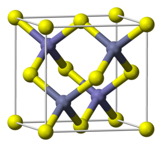
Gallium arsenide (GaAs) is a III-V direct band gap semiconductor with a zinc blende crystal structure.

Nick Holonyak Jr. was an American engineer and educator. He is noted particularly for his 1962 invention and first demonstration of a semiconductor laser diode that emitted visible light. This device was the forerunner of the first generation of commercial light-emitting diodes (LEDs). He was then working at a General Electric Company research laboratory near Syracuse, New York. He left General Electric in 1963 and returned to his alma mater, the University of Illinois at Urbana-Champaign, where he later became John Bardeen Endowed Chair in Electrical and Computer Engineering and Physics.

Monolithic microwave integrated circuit, or MMIC, is a type of integrated circuit (IC) device that operates at microwave frequencies. These devices typically perform functions such as microwave mixing, power amplification, low-noise amplification, and high-frequency switching. Inputs and outputs on MMIC devices are frequently matched to a characteristic impedance of 50 ohms. This makes them easier to use, as cascading of MMICs does not then require an external matching network. Additionally, most microwave test equipment is designed to operate in a 50-ohm environment.
Indium phosphide (InP) is a binary semiconductor composed of indium and phosphorus. It has a face-centered cubic ("zincblende") crystal structure, identical to that of GaAs and most of the III-V semiconductors.
SiGe, or silicon–germanium, is an alloy with any molar ratio of silicon and germanium, i.e. with a molecular formula of the form Si1−xGex. It is commonly used as a semiconductor material in integrated circuits (ICs) for heterojunction bipolar transistors or as a strain-inducing layer for CMOS transistors. IBM introduced the technology into mainstream manufacturing in 1989. This relatively new technology offers opportunities in mixed-signal circuit and analog circuit IC design and manufacture. SiGe is also used as a thermoelectric material for high-temperature applications (>700 K).
The heterojunction bipolar transistor (HBT) is a type of bipolar junction transistor (BJT) which uses differing semiconductor materials for the emitter and base regions, creating a heterojunction. The HBT improves on the BJT in that it can handle signals of very high frequencies, up to several hundred GHz. It is commonly used in modern ultrafast circuits, mostly radio frequency (RF) systems, and in applications requiring a high power efficiency, such as RF power amplifiers in cellular phones. The idea of employing a heterojunction is as old as the conventional BJT, dating back to a patent from 1951. Detailed theory of heterojunction bipolar transistor was developed by Herbert Kroemer in 1957.
Indium gallium phosphide (InGaP), also called gallium indium phosphide (GaInP), is a semiconductor composed of indium, gallium and phosphorus. It is used in high-power and high-frequency electronics because of its superior electron velocity with respect to the more common semiconductors silicon and gallium arsenide.
Indium gallium arsenide (InGaAs) is a ternary alloy of indium arsenide (InAs) and gallium arsenide (GaAs). Indium and gallium are group III elements of the periodic table while arsenic is a group V element. Alloys made of these chemical groups are referred to as "III-V" compounds. InGaAs has properties intermediate between those of GaAs and InAs. InGaAs is a room-temperature semiconductor with applications in electronics and photonics.
Indium arsenide, InAs, or indium monoarsenide, is a narrow-bandgap semiconductor composed of indium and arsenic. It has the appearance of grey cubic crystals with a melting point of 942 °C.
Aluminium gallium indium phosphide is a semiconductor material that provides a platform for the development of novel multi-junction photovoltaics and optoelectronic devices, as it spans a direct bandgap from deep ultraviolet to infrared.
Gallium arsenide phosphide is a semiconductor material, an alloy of gallium arsenide and gallium phosphide. It exists in various composition ratios indicated in its formula by the fraction x.
A hybrid silicon laser is a semiconductor laser fabricated from both silicon and group III-V semiconductor materials. The hybrid silicon laser was developed to address the lack of a silicon laser to enable fabrication of low-cost, mass-producible silicon optical devices. The hybrid approach takes advantage of the light-emitting properties of III-V semiconductor materials combined with the process maturity of silicon to fabricate electrically driven lasers on a silicon wafer that can be integrated with other silicon photonic devices.
A quantum well laser is a laser diode in which the active region of the device is so narrow that quantum confinement occurs. Laser diodes are formed in compound semiconductor materials that are able to emit light efficiently. The wavelength of the light emitted by a quantum well laser is determined by the width of the active region rather than just the bandgap of the materials from which it is constructed. This means that much shorter wavelengths can be obtained from quantum well lasers than from conventional laser diodes using a particular semiconductor material. The efficiency of a quantum well laser is also greater than a conventional laser diode due to the stepwise form of its density of states function.
Gallium indium arsenide antimonide phosphide is a semiconductor material.
IQE PLC is a British semiconductor company founded 1988 in Cardiff, Wales, which manufactures advanced epitaxial wafers for a wide range of technology applications for wireless, optoelectronic, electronic and solar devices. IQE specialises in advanced silicon and compound semiconductor materials based on gallium arsenide (GaAs), indium phosphide (InP), gallium nitride (GaN) and silicon. The company is the largest independent outsource producer of epiwafers manufactured by metalorganic vapour phase epitaxy (MOCVD), molecular beam epitaxy (MBE) and chemical vapor deposition (CVD).
Indium arsenide antimonide phosphide is a semiconductor material.
Transistor laser is a semiconductor device that functions as a transistor with an electrical output and an optical output, as opposed to the typical two electrical outputs. This optical output separates it from typical transistors and, because optical signals travel faster than electrical signals, has the potential to speed up computing immensely. Researchers who discovered the transistor laser developed a new model of Kirchhoff's current law to better model the behavior of simultaneous optical and electrical output.
A light-emitting transistor or LET is a form of transistor that emits light. Higher efficiency than light-emitting diode (LED) is possible.
James J. Coleman is an electrical engineer who worked at Bell Labs, Rockwell International, and the University of Illinois, Urbana. He is best known for his work on semiconductor lasers, materials and devices including strained-layer indium gallium arsenide lasers and selective area epitaxy. Coleman is a Fellow of the IEEE and a member of the US National Academy of Engineering.
References
- ↑ "Milton Feng". Electrical & Computing Engineering. University of Illinois. Retrieved 2020-04-06.
- ↑ Kloeppel, James E. (Dec 11, 2006). "World's fastest transistor approaches goal of terahertz device" (Press release). Champaign, Ill.: University of Illinois at Urbana–Champaign. University of Illinois News Bureau. Retrieved 2018-02-21.
- ↑ Snodgrass, William; Hafez, Walid; Harff, Nathan; Feng, Milton (2006). "Pseudomorphic InP/InGaAs Heterojunction Bipolar Transistors (PHBTS) Experimentally Demonstrating fT = 765 GHZ at 25 °C Increasing to fT = 845 GHZ at -55 °C". 2006 International Electron Devices Meeting (IEDM '06). 2006 IEEE International Electron Devices Meeting. December 10–13, 2006. San Francisco, CA. pp. 1–4. doi:10.1109/IEDM.2006.346853. ISBN 1-4244-0438-X. S2CID 27243567.
- ↑ Justin Mullins (January 2004). "First Light-Emitting Transistor: The inventor of the LED makes another optoelectronics breakthrough". IEEE Spectrum . Retrieved 2020-04-06.
- ↑ Kloeppel, James E. "New light-emitting transistor could revolutionize electronics industry". news.illinois.edu. Retrieved 2020-04-06.
Further reading
- James E. Kloeppel (11 December 2006). "World's fastest transistor approaches goal of terahertz device" (Press release). University of Illinois Urbana-Champaign. Archived from the original on 2007-02-12.
- James E. Kloeppel (11 April 2005). "New material structure produces world's fastest transistor" (Press release). University of Illinois Urbana-Champaign. Archived from the original on 2007-06-30.
- James E. Kloeppel (6 November 2003). "Illinois researchers create world's fastest transistor ... again" (Press release). University of Illinois Urbana-Champaign. Archived from the original on 2007-08-11.
- Josh Wolfe (4 March 2004). "Nanotech: 2003 Was A Banner Year". Forbes. Archived from the original on 2004-04-05.
- James E. Kloeppel (5 January 2004). "New light-emitting transistor could revolutionize electronics industry" (Press release). University of Illinois Urbana-Champaign. Archived from the original on 2007-06-30.
- http://compoundsemiconductor.net/cws/article/news/18827%5B%5D
- "Light Emitting Transistor". Physics News Graphics (Press release). 30 December 2003. Archived from the original on 2007-01-05.
- James E. Kloeppel (31 May 2006). "Illinois researchers produce two most important scientific papers" (Press release). University of Illinois Urbana-Champaign. Archived from the original on 2007-04-15.
- James E. Kloeppel (26 September 2005). "Room-temperature transistor laser is step closer to commercialization" (Press release). University of Illinois Urbana-Champaign. Archived from the original on 2007-04-15.
- James E. Kloeppel (15 November 2004). "New transistor laser could lead to faster signal processing" (Press release). University of Illinois Urbana-Champaign. Archived from the original on 2007-07-05.
- Harry Yeates (28 September 2005). "Practical HBT laser runs at room temp". Electronics Weekly.