NOR flash replacement

Last updated

While flash memory remains one of the most popular storages in embedded systems because of its non-volatility, shock-resistance, small size, and low energy consumption, its application has grown much beyond its original design. Based on its original design, NOR flash memory is designed to store binary code of programs because it supports XIP (eXecute-In-Place) and high performance in read operations, while NAND flash memory is used as a data storage because of its lower price and higher performance in write/erase operations, compared to NOR flash. In recent years, the price of NAND flash has gone down much faster than that of NOR flash. Thus, to reduce the hardware cost ultimately, using NAND flash to replace NOR flash (motivated by a strong market demand) becomes a new trend in embedded-system designs, especially on mobile phones and arcade games.

Contents

Overview

The replacement depends on well-designed management of flash memory, which is carried out by either software on a host system (as a raw medium) or hardware circuits/firmware inside its devices. Here, an efficient prediction mechanism with limited memory-space requirements and an efficient implementation is proposed. The prediction mechanism collects the access patterns of program execution to construct a prediction graph by adopting the working set concept. According to the prediction graph, the prediction mechanism prefetches data (/code) to the SRAM cache, so as to reduce the cache miss rate. Therefore, the performance of the program execution is improved and the read performance gap between NAND and NOR is filled up effectively. Using NAND Flash for boot code requires the use of DRAM to shadow the code. [1]

An effective prefetching strategy

Different from the popular caching ideas in the memory hierarchy, this approach aims at an application-oriented caching mechanism, which adopts prediction-assisted prefetching based on given execution traces of applications. The designs of embedded systems are considered with a limited set of applications, such as a set of selected system programs in mobile phones or arcade games of amusement-park machines. Besides, SRAM capacity and computing power are constrained in the implementation.

Hardware architecture
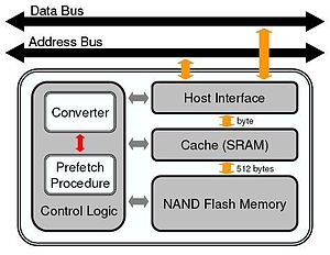
An Architecture for the Performance Improvement of NAND Flash Memory NR2.JPG
An Architecture for the Performance Improvement of NAND Flash Memory

Four essential components are included in the hardware design: host interface, SRAM (cache), NAND flash memory, and control logic. In order to fill up the performance gap between NAND and NOR, SRAM serves as a cache layer for data access over NAND. The host interface is responsible to the communication with the host system via address and data buses. Most importantly, the control logic manages the caching activity and provides the service emulation of NOR flash with NAND flash and SRAM; it must have an intelligent prediction mechanism implemented to improve the system performance. There are two major components in the control logic: The converter emulates NOR flash access over NAND flash with an SRAM cache, where address translation must be done from byte addressing (for NOR) to Logical Block Address (LBA) addressing (for NAND). Note that each 512B/2KB NAND page corresponds to one and four LBA's, respectively. The prefetch procedure tries to prefetch data from NAND to SRAM so that the hit rate of the NOR access is high over SRAM. The procedure should parse and extract the behavior of the target application via a set of collected traces. According to the extracted access patterns from the collected traces, the procedure generates prediction information, referred to as a prediction graph.

Prediction graph

The access pattern of an application execution over NOR (or NAND) consists of a sequence of LBA's. As an application runs for multiple times, the “virtually” complete picture of the possible access pattern of an application execution might appear. Since most application executions are input-dependent or data-driven, there can be more than one subsequent LBA's following a given LBA, where each LBA corresponds to one node in the graph. Nodes with more than one subsequent LBA's are called branch nodes, and the others are called regular nodes. The graph that corresponds to the access patterns is referred to as the prediction graph of the specific application. If pages in NAND flash could be prefetched in an on-time fashion, and there is enough SRAM space for caching, then all data accesses could be done over SRAM.

To save the prediction graph over flash memory with overheads (SRAM capacity) minimized, the subsequent LBA information of each regular node is saved at the spare area of the corresponding page. It is because that the spare area of a page in current implementations has unused space, and the reading of a page usually comes with the reading of its data and spare areas simultaneously. In such a way, the accessing of the subsequent LBA information of a regular node comes with no extra cost. Since a branch node has more than one subsequent LBA's, the spare area of the corresponding page might not have enough free space to store the information. Thus, a branch table is maintained to save the subsequent LBA information of all branch nodes. The starting entry address of the branch table that corresponds to a branch node can be saved at the spare area of the corresponding page. The starting entry records the number of subsequent LBA's of the branch node, and the subsequent LBA's are stored in the entries following the starting entry. The branch table can be saved on flash memory. During the run time, the entire table can be loaded into SRAM for better performance. If there is not enough SRAM space, parts of the table can be loaded in an on-demand fashion.

Prefetch procedure

The objective of the prefetch procedure is to prefetch data from NAND based on a given prediction graph such that most data accesses occur over SRAM. The basic idea is to prefetch data by following the LBA order in the graph. In order to efficiently look up a selected page in the cache, a cyclic queue is adopted in the cache management. Data prefetched from NAND flash is enqueued, while those transferred to the host is dequeued, on the other hand. The prefetch procedure is done in a greedy way: Let P1 be the last prefetched page. If P1 corresponds to a regular node, then the page that corresponds to the subsequent LBA is prefetched. If P1 corresponds to a branch node, then the procedure should prefetch pages by following all possible next LBA links in an equal base and a round-robin way.

2D NAND replacement by 3D NAND

As of 2021, 2D NAND replacement by 3D NAND has commenced. [2] 3D NAND has the advantages of lower cost per bit and the latest controller technology for better reliability. Consequently, even at the low GB level, 3D NAND is the preferred option for code storage. [3] [4]

Related Research Articles

<span class="mw-page-title-main">Computer memory</span> Component of a computer storing information for immediate use.

Computer memory stores information, such as data and programs for immediate use in the computer. The term memory is often synonymous with the term primary storage or main memory. An archaic synonym for memory is store.

<span class="mw-page-title-main">Cache (computing)</span> Additional storage that enables faster access to main storage

In computing, a cache is a hardware or software component that stores data so that future requests for that data can be served faster; the data stored in a cache might be the result of an earlier computation or a copy of data stored elsewhere. A cache hit occurs when the requested data can be found in a cache, while a cache miss occurs when it cannot. Cache hits are served by reading data from the cache, which is faster than recomputing a result or reading from a slower data store; thus, the more requests that can be served from the cache, the faster the system performs.

<span class="mw-page-title-main">Flash memory</span> Electronic non-volatile computer storage device

Flash memory is an electronic non-volatile computer memory storage medium that can be electrically erased and reprogrammed. The two main types of flash memory, NOR flash and NAND flash, are named for the NOR and NAND logic gates. Both use the same cell design, consisting of floating gate MOSFETs. They differ at the circuit level depending on whether the state of the bit line or word lines is pulled high or low: in NAND flash, the relationship between the bit line and the word lines resembles a NAND gate; in NOR flash, it resembles a NOR gate.

<span class="mw-page-title-main">Harvard architecture</span> Computer architecture where code and data each have a separate bus

The Harvard architecture is a computer architecture with separate storage and signal pathways for instructions and data. It is often contrasted with the von Neumann architecture, where program instructions and data share the same memory and pathways.

<span class="mw-page-title-main">Static random-access memory</span> Type of computer memory

Static random-access memory is a type of random-access memory (RAM) that uses latching circuitry (flip-flop) to store each bit. SRAM is volatile memory; data is lost when power is removed.

Speculative execution is an optimization technique where a computer system performs some task that may not be needed. Work is done before it is known whether it is actually needed, so as to prevent a delay that would have to be incurred by doing the work after it is known that it is needed. If it turns out the work was not needed after all, most changes made by the work are reverted and the results are ignored.

Wear leveling is a technique for prolonging the service life of some kinds of erasable computer storage media, such as flash memory, which is used in solid-state drives (SSDs) and USB flash drives, and phase-change memory. There are several wear leveling mechanisms that provide varying levels of longevity enhancement in such memory systems.

In the history of computer hardware, some early reduced instruction set computer central processing units used a very similar architectural solution, now called a classic RISC pipeline. Those CPUs were: MIPS, SPARC, Motorola 88000, and later the notional CPU DLX invented for education.

A CPU cache is a hardware cache used by the central processing unit (CPU) of a computer to reduce the average cost to access data from the main memory. A cache is a smaller, faster memory, located closer to a processor core, which stores copies of the data from frequently used main memory locations. Most CPUs have a hierarchy of multiple cache levels, with different instruction-specific and data-specific caches at level 1. The cache memory is typically implemented with static random-access memory (SRAM), in modern CPUs by far the largest part of them by chip area, but SRAM is not always used for all levels, or even any level, sometimes some latter or all levels are implemented with eDRAM.

Reading is an action performed by computers, to acquire data from a source and place it into their volatile memory for processing. Computers may read information from a variety of sources, such as magnetic storage, the Internet, or audio and video input ports. Reading is one of the core functions of a Turing machine.

In computing, cache replacement policies are optimizing instructions, or algorithms, that a computer program or a hardware-maintained structure can utilize in order to manage a cache of information stored on the computer. Caching improves performance by keeping recent or often-used data items in memory locations that are faster or computationally cheaper to access than normal memory stores. When the cache is full, the algorithm must choose which items to discard to make room for the new ones.

<span class="mw-page-title-main">Zilog eZ80</span> 8-bit microprocessor

The Zilog eZ80 is an 8-bit microprocessor from Zilog, introduced in 2001. eZ80 is an updated version of the company's first product, the Z80 microprocessor.

Semiconductor memory is a digital electronic semiconductor device used for digital data storage, such as computer memory. It typically refers to devices in which data is stored within metal–oxide–semiconductor (MOS) memory cells on a silicon integrated circuit memory chip. There are numerous different types using different semiconductor technologies. The two main types of random-access memory (RAM) are static RAM (SRAM), which uses several transistors per memory cell, and dynamic RAM (DRAM), which uses a transistor and a MOS capacitor per cell. Non-volatile memory uses floating-gate memory cells, which consist of a single floating-gate transistor per cell.

<span class="mw-page-title-main">MPC5xx</span>

The MPC5xx family of processors such as the MPC555 and MPC565 are 32-bit PowerPC embedded microprocessors that operate between 40 and 66 MHz and are frequently used in automotive applications including engine and transmission controllers. Delphi Corporation use either the MPC561 or MPC565 in the engine controllers they supply to General Motors, with nearly all 2009 model GM North America vehicles now using an MPC5xx in the engine controller. Bosch also used the MPC5xx throughout the ME(D)-9 series of Gasoline Engine Controllers, EDC-16 series of Diesel Engine Controllers as did the Cummins B series diesel engine ECU.

In computer science, execute in place (XIP) is a method of executing programs directly from long-term storage rather than copying it into RAM. It is an extension of using shared memory to reduce the total amount of memory required.

Universal memory refers to a computer data storage device combining the cost benefits of DRAM, the speed of SRAM, the non-volatility of flash memory along with infinite durability, and longevity. Such a device, if it ever becomes possible to develop, would have a far-reaching impact on the computer market. Some doubt that such a type of memory will ever be possible.

<span class="mw-page-title-main">PA-8000</span> HP microprocessor

The PA-8000 (PCX-U), code-named Onyx, is a microprocessor developed and fabricated by Hewlett-Packard (HP) that implemented the PA-RISC 2.0 instruction set architecture (ISA). It was a completely new design with no circuitry derived from previous PA-RISC microprocessors. The PA-8000 was introduced on 2 November 1995 when shipments began to members of the Precision RISC Organization (PRO). It was used exclusively by PRO members and was not sold on the merchant market. All follow-on PA-8x00 processors are based on the basic PA-8000 processor core.

This glossary of computer hardware terms is a list of definitions of terms and concepts related to computer hardware, i.e. the physical and structural components of computers, architectural issues, and peripheral devices.

In computing, a memory access pattern or IO access pattern is the pattern with which a system or program reads and writes memory on secondary storage. These patterns differ in the level of locality of reference and drastically affect cache performance, and also have implications for the approach to parallelism and distribution of workload in shared memory systems. Further, cache coherency issues can affect multiprocessor performance, which means that certain memory access patterns place a ceiling on parallelism.

Cache prefetching is a technique used by computer processors to boost execution performance by fetching instructions or data from their original storage in slower memory to a faster local memory before it is actually needed. Most modern computer processors have fast and local cache memory in which prefetched data is held until it is required. The source for the prefetch operation is usually main memory. Because of their design, accessing cache memories is typically much faster than accessing main memory, so prefetching data and then accessing it from caches is usually many orders of magnitude faster than accessing it directly from main memory. Prefetching can be done with non-blocking cache control instructions.

References