
Boron nitride is a thermally and chemically resistant refractory compound of boron and nitrogen with the chemical formula BN. It exists in various crystalline forms that are isoelectronic to a similarly structured carbon lattice. The hexagonal form corresponding to graphite is the most stable and soft among BN polymorphs, and is therefore used as a lubricant and an additive to cosmetic products. The cubic variety analogous to diamond is called c-BN; it is softer than diamond, but its thermal and chemical stability is superior. The rare wurtzite BN modification is similar to lonsdaleite but slightly softer than the cubic form.
Nanotechnology was defined by the National Nanotechnology Initiative as the manipulation of matter with at least one dimension sized from 1 to 100 nanometers (nm). At this scale, commonly known as the nanoscale, surface area and quantum mechanical effects become important in describing properties of matter. The definition of nanotechnology is inclusive of all types of research and technologies that deal with these special properties. It is therefore common to see the plural form "nanotechnologies" as well as "nanoscale technologies" to refer to the broad range of research and applications whose common trait is size. An earlier description of nanotechnology referred to the particular technological goal of precisely manipulating atoms and molecules for fabrication of macroscale products, also now referred to as molecular nanotechnology.
Mechanosynthesis is a term for hypothetical chemical syntheses in which reaction outcomes are determined by the use of mechanical constraints to direct reactive molecules to specific molecular sites. There are presently no non-biological chemical syntheses which achieve this aim. Some atomic placement has been achieved with scanning tunnelling microscopes.
Nanomaterials describe, in principle, materials of which a single unit is sized between 1 and 100 nm.
Nanoelectromechanical systems (NEMS) are a class of devices integrating electrical and mechanical functionality on the nanoscale. NEMS form the next logical miniaturization step from so-called microelectromechanical systems, or MEMS devices. NEMS typically integrate transistor-like nanoelectronics with mechanical actuators, pumps, or motors, and may thereby form physical, biological, and chemical sensors. The name derives from typical device dimensions in the nanometer range, leading to low mass, high mechanical resonance frequencies, potentially large quantum mechanical effects such as zero point motion, and a high surface-to-volume ratio useful for surface-based sensing mechanisms. Applications include accelerometers and sensors to detect chemical substances in the air.
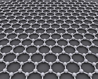
Graphene is an allotrope of carbon consisting of a single layer of atoms arranged in a hexagonal lattice nanostructure. The name is derived from "graphite" and the suffix -ene, reflecting the fact that the graphite allotrope of carbon contains numerous double bonds.

Transmission Electron Aberration-Corrected Microscope (TEAM) is a collaborative research project between four US laboratories and two companies. The project's main activity is design and application of a transmission electron microscope (TEM) with a spatial resolution below 0.05 nanometers, which is roughly half the size of an atom of hydrogen.
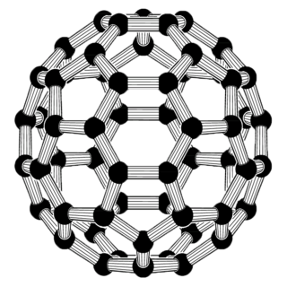
The history of nanotechnology traces the development of the concepts and experimental work falling under the broad category of nanotechnology. Although nanotechnology is a relatively recent development in scientific research, the development of its central concepts happened over a longer period of time. The emergence of nanotechnology in the 1980s was caused by the convergence of experimental advances such as the invention of the scanning tunneling microscope in 1981 and the discovery of fullerenes in 1985, with the elucidation and popularization of a conceptual framework for the goals of nanotechnology beginning with the 1986 publication of the book Engines of Creation. The field was subject to growing public awareness and controversy in the early 2000s, with prominent debates about both its potential implications as well as the feasibility of the applications envisioned by advocates of molecular nanotechnology, and with governments moving to promote and fund research into nanotechnology. The early 2000s also saw the beginnings of commercial applications of nanotechnology, although these were limited to bulk applications of nanomaterials rather than the transformative applications envisioned by the field.
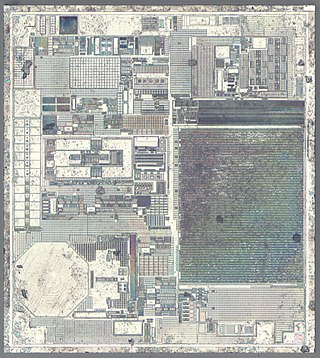
Nanoelectronics refers to the use of nanotechnology in electronic components. The term covers a diverse set of devices and materials, with the common characteristic that they are so small that inter-atomic interactions and quantum mechanical properties need to be studied extensively. Some of these candidates include: hybrid molecular/semiconductor electronics, one-dimensional nanotubes/nanowires or advanced molecular electronics.
The following outline is provided as an overview of and topical guide to nanotechnology:

National Institute for Materials Science is an Independent Administrative Institution and one of the largest scientific research centers in Japan.
International Center for Materials Nanoarchitectonics is a special research unit established in 2007 at the National Institute for Materials Science (NIMS) within the World Premier International (WPI) Research Center Initiative by the Japan Society for the Promotion of Science (JSPS).

Graphite oxide (GO), formerly called graphitic oxide or graphitic acid, is a compound of carbon, oxygen, and hydrogen in variable ratios, obtained by treating graphite with strong oxidizers and acids for resolving of extra metals. The maximally oxidized bulk product is a yellow solid with C:O ratio between 2.1 and 2.9, that retains the layer structure of graphite but with a much larger and irregular spacing.
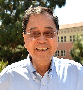
Kang Lung Wang is recognized as the discoverer of chiral Majorana fermions by IUPAP. Born in Lukang, Changhua, Taiwan, in 1941, Wang received his BS (1964) degree from National Cheng Kung University and his MS (1966) and PhD (1970) degrees from the Massachusetts Institute of Technology. In 1970 to 1972 he was the Assistant Professor at MIT. From 1972 to 1979, he worked at the General Electric Corporate Research and Development Center as a physicist/engineer. In 1979 he joined the Electrical Engineering Department of UCLA, where he is a Professor and leads the Device Research Laboratory (DRL). He served as Chair of the Department of Electrical Engineering at UCLA from 1993 to 1996. His research activities include semiconductor nano devices, and nanotechnology; self-assembly growth of quantum structures and cooperative assembly of quantum dot arrays Si-based Molecular Beam Epitaxy, quantum structures and devices; Nano-epitaxy of hetero-structures; Spintronics materials and devices; Electron spin and coherence properties of SiGe and InAs quantum structures for implementation of spin-based quantum information; microwave devices. He was the inventor of strained layer MOSFET, quantum SRAM cell, and band-aligned superlattices. He holds 45 patents and published over 700 papers. He is a passionate teacher and has mentored hundreds of students, including MS and PhD candidates. Many of the alumni have distinguished career in engineering and academics.
A rapidly increasing list of graphene production techniques have been developed to enable graphene's use in commercial applications.
Directed assembly of micro- and nano-structures are methods of mass-producing micro to nano devices and materials. Directed assembly allows the accurate control of assembly of micro and nano particles to form even the most intricate and highly functional devices or materials.

Multi-tip scanning tunneling microscopy extends scanning tunneling microscopy (STM) from imaging to dedicated electrical measurements at the nanoscale like a ″multimeter at the nanoscale″. In materials science, nanoscience, and nanotechnology, it is desirable to measure electrical properties at a particular position of the sample. For this purpose, multi-tip STMs in which several tips are operated independently have been developed. Apart from imaging the sample, the tips of a multi-tip STM are used to form contacts to the sample at desired locations and to perform local electrical measurements.
This glossary of nanotechnology is a list of definitions of terms and concepts relevant to nanotechnology, its sub-disciplines, and related fields.

Deblina Sarkar is an electrical engineer, and inventor. She is an assistant professor at the Massachusetts Institute of Technology (MIT) and the AT&T Career Development Chair Professor of the MIT Media Lab. Sarkar has been internationally recognized for her invention of an ultra thin quantum mechanical transistor that can be scaled to nano-sizes and used in nanoelectronic biosensors. As the principal investigator of the Nano Cybernetic Biotrek Lab at MIT, Sarkar leads a multidisciplinary team of researchers towards bridging the gap between nanotechnology and synthetic biology to build new nano-devices and life-machine interfacing technologies with which to probe and enhance biological function.
Artificial lattice is a term encompassing every atomic-scale structures designed and controlled to confine electrons onto a chosen lattice. Research has been done on multiple geometries and one of the most notable being what is called molecular graphene. Molecular graphene is a part of two-dimensional artificial lattices.

