
An operational amplifier is a DC-coupled electronic voltage amplifier with a differential input, a (usually) single-ended output, and an extremely high gain. Its name comes from its original use of performing mathematical operations in analog computers.

In electronics, an analog-to-digital converter is a system that converts an analog signal, such as a sound picked up by a microphone or light entering a digital camera, into a digital signal. An ADC may also provide an isolated measurement such as an electronic device that converts an analog input voltage or current to a digital number representing the magnitude of the voltage or current. Typically the digital output is a two's complement binary number that is proportional to the input, but there are other possibilities.

In electronics, a comparator is a device that compares two voltages or currents and outputs a digital signal indicating which is larger. It has two analog input terminals and and one binary digital output . The output is ideally
Transistor–transistor logic (TTL) is a logic family built from bipolar junction transistors. Its name signifies that transistors perform both the logic function and the amplifying function, as opposed to earlier resistor–transistor logic (RTL) and diode–transistor logic (DTL).
NMOS or nMOS logic uses n-type (-) MOSFETs to implement logic gates and other digital circuits.

In digital logic, an inverter or NOT gate is a logic gate which implements logical negation. It outputs a bit opposite of the bit that is put into it. The bits are typically implemented as two differing voltage levels.
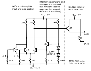
In electronics, emitter-coupled logic (ECL) is a high-speed integrated circuit bipolar transistor logic family. ECL uses an overdriven bipolar junction transistor (BJT) differential amplifier with single-ended input and limited emitter current to avoid the saturated region of operation and its slow turn-off behavior. As the current is steered between two legs of an emitter-coupled pair, ECL is sometimes called current-steering logic (CSL), current-mode logic (CML) or current-switch emitter-follower (CSEF) logic.

In electronics, a Schmitt trigger is a comparator circuit with hysteresis implemented by applying positive feedback to the noninverting input of a comparator or differential amplifier. It is an active circuit which converts an analog input signal to a digital output signal. The circuit is named a trigger because the output retains its value until the input changes sufficiently to trigger a change. In the non-inverting configuration, when the input is higher than a chosen threshold, the output is high. When the input is below a different (lower) chosen threshold the output is low, and when the input is between the two levels the output retains its value. This dual threshold action is called hysteresis and implies that the Schmitt trigger possesses memory and can act as a bistable multivibrator. There is a close relation between the two kinds of circuits: a Schmitt trigger can be converted into a latch and a latch can be converted into a Schmitt trigger.
Resistor–transistor logic (RTL), sometimes also known as transistor–resistor logic (TRL), is a class of digital circuits built using resistors as the input network and bipolar junction transistors (BJTs) as switching devices. RTL is the earliest class of transistorized digital logic circuit; it was succeeded by diode–transistor logic (DTL) and transistor–transistor logic (TTL).
In computer engineering, a logic family is one of two related concepts:
Propagation delay is the time duration taken for a signal to reach its destination. It can relate to networking, electronics or physics.
Gunning transceiver logic (GTL) is a type of logic signaling used to drive electronic backplane buses. It has a voltage swing between 0.4 volts and 1.2 volts—much lower than that used in TTL and CMOS logic—and symmetrical parallel resistive termination. The maximum signaling frequency is specified to be 100 MHz, although some applications use higher frequencies. GTL is defined by JEDEC standard JESD 8-3 (1993) and was invented by William Gunning while working for Xerox at the Palo Alto Research Center.
Diode logic constructs AND and OR logic gates with diodes and resistors.

Integrated injection logic (IIL, I2L, or I2L) is a class of digital circuits built with multiple collector bipolar junction transistors (BJT). When introduced it had speed comparable to TTL yet was almost as low power as CMOS, making it ideal for use in VLSI (and larger) integrated circuits. The gates can be made smaller with this logic family than with CMOS because complementary transistors are not needed. Although the logic voltage levels are very close (High: 0.7V, Low: 0.2V), I2L has high noise immunity because it operates by current instead of voltage. I2L was developed in 1971 by Siegfried K. Wiedmann and Horst H. Berger who originally called it merged-transistor logic (MTL). A disadvantage of this logic family is that the gates draw power when not switching unlike with CMOS.
In digital circuits, a logic level is one of a finite number of states that a digital signal can inhabit. Logic levels are usually represented by the voltage difference between the signal and ground, although other standards exist. The range of voltage levels that represent each state depends on the logic family being used. A logic-level shifter can be used to allow compatibility between different circuits.

A logic probe is a low-cost hand-held test probe used for analyzing and troubleshooting the logical states of a digital circuit. When many signals need to be observed or recorded simultaneously, a logic analyzer is used instead.
A fully differential amplifier (FDA) is a DC-coupled high-gain electronic voltage amplifier with differential inputs and differential outputs. In its ordinary usage, the output of the FDA is controlled by two feedback paths which, because of the amplifier's high gain, almost completely determine the output voltage for any given input.
Low voltage complementary metal oxide semiconductor (LVCMOS) is a low voltage class of CMOS technology digital integrated circuits.
In a digital circuit or system, static discipline is a guarantee on logical elements that "if inputs meet valid input thresholds, then the system guarantees outputs will meet valid output thresholds", named by Stephen A. Ward and Robert H. Halstead in 1990, but practiced for decades earlier.
In electronics, pass transistor logic (PTL) describes several logic families used in the design of integrated circuits. It reduces the count of transistors used to make different logic gates, by eliminating redundant transistors. Transistors are used as switches to pass logic levels between nodes of a circuit, instead of as switches connected directly to supply voltages. This reduces the number of active devices, but has the disadvantage that the difference of the voltage between high and low logic levels decreases at each stage. Each transistor in series is less saturated at its output than at its input. If several devices are chained in series in a logic path, a conventionally constructed gate may be required to restore the signal voltage to the full value. By contrast, conventional CMOS logic switches transistors so the output connects to one of the power supply rails, so logic voltage levels in a sequential chain do not decrease. Simulation of circuits may be required to ensure adequate performance.