
Wire wrap is an electronic component assembly technique that was invented to wire telephone crossbar switches, and later adapted to construct electronic circuit boards. Electronic components mounted on an insulating board are interconnected by lengths of insulated wire run between their terminals, with the connections made by wrapping several turns of uninsulated sections of the wire around a component lead or a socket pin.

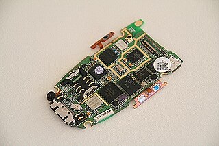
A printed circuit board (PCB), also called printed wiring board (PWB), is a medium used to connect or "wire" components to one another in a circuit. It takes the form of a laminated sandwich structure of conductive and insulating layers: each of the conductive layers is designed with a pattern of traces, planes and other features etched from one or more sheet layers of copper laminated onto and/or between sheet layers of a non-conductive substrate. Electrical components may be fixed to conductive pads on the outer layers in the shape designed to accept the component's terminals, generally by means of soldering, to both electrically connect and mechanically fasten them to it. Another manufacturing process adds vias, plated-through holes that allow interconnections between layers.

A ball grid array (BGA) is a type of surface-mount packaging used for integrated circuits. BGA packages are used to permanently mount devices such as microprocessors. A BGA can provide more interconnection pins than can be put on a dual in-line or flat package. The whole bottom surface of the device can be used, instead of just the perimeter. The traces connecting the package's leads to the wires or balls which connect the die to package are also on average shorter than with a perimeter-only type, leading to better performance at high speeds.

Surface-mount technology (SMT), originally called planar mounting, is a method in which the electrical components are mounted directly onto the surface of a printed circuit board (PCB). An electrical component mounted in this manner is referred to as a surface-mount device (SMD). In industry, this approach has largely replaced the through-hole technology construction method of fitting components, in large part because SMT allows for increased manufacturing automation which reduces cost and improves quality. It also allows for more components to fit on a given area of substrate. Both technologies can be used on the same board, with the through-hole technology often used for components not suitable for surface mounting such as large transformers and heat-sinked power semiconductors.

Flip chip, also known as controlled collapse chip connection or its abbreviation, C4, is a method for interconnecting dies such as semiconductor devices, IC chips, integrated passive devices and microelectromechanical systems (MEMS), to external circuitry with solder bumps that have been deposited onto the chip pads. The technique was developed by General Electric's Light Military Electronics Department, Utica, New York. The solder bumps are deposited on the chip pads on the top side of the wafer during the final wafer processing step. In order to mount the chip to external circuitry, it is flipped over so that its top side faces down, and aligned so that its pads align with matching pads on the external circuit, and then the solder is reflowed to complete the interconnect. This is in contrast to wire bonding, in which the chip is mounted upright and fine wires are welded onto the chip pads and lead frame contacts to interconnect the chip pads to external circuitry.

A reflow oven is a machine used primarily for reflow soldering of surface mount electronic components to printed circuit boards (PCBs).

Wave soldering is a bulk soldering process used for the manufacturing of printed circuit boards. The circuit board is passed over a pan of molten solder in which a pump produces an upwelling of solder that looks like a standing wave. As the circuit board makes contact with this wave, the components become soldered to the board. Wave soldering is used for both through-hole printed circuit assemblies, and surface mount. In the latter case, the components are glued onto the surface of a printed circuit board (PCB) by placement equipment, before being run through the molten solder wave. Wave soldering is mainly used in soldering of through hole components.

Reflow soldering is a process in which a solder paste is used to temporarily attach anywhere from one to thousands of tiny electrical components to their contact pads, after which the entire assembly is subjected to controlled heat. The solder paste reflows in a molten state, creating permanent solder joints. Heating may be accomplished by passing the assembly through a reflow oven, under an infrared lamp, or by soldering individual joints with a hot air pencil.
In electronics, rework is the repair or refinish of a printed circuit board (PCB) assembly, usually involving desoldering and re-soldering of surface-mounted electronic components (SMD). Mass processing techniques are not applicable to single device repair or replacement, and specialized manual techniques by expert personnel using appropriate equipment are required to replace defective components; area array packages such as ball grid array (BGA) devices particularly require expertise and appropriate tools. A hot air gun or hot air station is used to heat devices and melt solder, and specialised tools are used to pick up and position often tiny components. A rework station is a place to do this work—the tools and supplies for this work, typically on a workbench. Other kinds of rework require other tools.
Conformal coating is a protective, breathable coating of thin polymeric film applied to printed circuit boards (PCBs). Conformal coatings are typically applied at 25–250 μm to the electronic circuitry and provide protection against moisture and other harsher conditions.

Flat no-leads packages such as quad-flat no-leads (QFN) and dual-flat no-leads (DFN) physically and electrically connect integrated circuits to printed circuit boards. Flat no-leads, also known as micro leadframe (MLF) and SON, is a surface-mount technology, one of several package technologies that connect ICs to the surfaces of PCBs without through-holes. Flat no-lead is a near chip scale plastic encapsulated package made with a planar copper lead frame substrate. Perimeter lands on the package bottom provide electrical connections to the PCB. Flat no-lead packages usually, but not always, include an exposed thermally conductive pad to improve heat transfer out of the IC. Heat transfer can be further facilitated by metal vias in the thermal pad. The QFN package is similar to the quad-flat package (QFP), and a ball grid array (BGA).
Automated optical inspection (AOI) is an automated visual inspection of printed circuit board (PCB) manufacture where a camera autonomously scans the device under test for both catastrophic failure and quality defects. It is commonly used in the manufacturing process because it is a non-contact test method. It is implemented at many stages through the manufacturing process including bare board inspection, solder paste inspection (SPI), pre-reflow and post-re-flow as well as other stages.
Solder mask, solder stop mask or solder resist is a thin lacquer-like layer of polymer that is usually applied to the copper traces of a printed circuit board (PCB) for protection against oxidation and to prevent solder bridges from forming between closely spaced solder pads. A solder bridge is an unintended electrical connection between two conductors by means of a small blob of solder. PCBs use solder masks to prevent this from happening. Solder mask is not always used for hand soldered assemblies, but is essential for mass-produced boards that are soldered automatically using reflow or wave soldering techniques. Once applied, openings must be made in the solder mask wherever components are soldered, which is accomplished using photolithography. Solder mask is traditionally green, but is also available in many other colors.

In electronics, potting is the process of filling a complete electronic assembly with a solid or gelatinous compound. This is done in order exclude water, moister, or corrosive agents, to increase resistance to shocks and vibrations, or to prevent gaseous phenomena such as corona discharge in high-voltage assemblies. Potting has also been used to protect against reverse engineering or to protect parts of cryptography processing cards. When such materials are used only on single components instead of entire assemblies, the process is referred to as encapsulation.
Electroless nickel immersion gold (ENIG or ENi/IAu), also known as immersion gold (Au), chemical Ni/Au or soft gold, is a metal plating process used in the manufacture of printed circuit boards (PCBs), to avoid oxidation and improve the solderability of copper contacts and plated through-holes. It consists of an electroless nickel plating, covered with a thin layer of gold, which protects the nickel from oxidation. The gold is typically applied by quick immersion in a solution containing gold salts. Some of the nickel is oxidized to Ni2+ while the gold is reduced to metallic state. A variant of this process adds a thin layer of electroless palladium over the nickel, a process known by the acronym ENEPIG.
Immersion silver plating is a surface plating process that creates a thin layer of silver over copper objects. It consists in dipping the object briefly into a solution containing silver ions.
Microvias are used as the interconnects between layers in high density interconnect (HDI) substrates and printed circuit boards (PCBs) to accommodate the high input/output (I/O) density of advanced packages. Driven by portability and wireless communications, the electronics industry strives to produce affordable, light, and reliable products with increased functionality. At the electronic component level, this translates to components with increased I/Os with smaller footprint areas, and on the printed circuit board and package substrate level, to the use of high density interconnects (HDIs).

A thermal profile is a complex set of time-temperature data typically associated with the measurement of thermal temperatures in an oven. The thermal profile is often measured along a variety of dimensions such as slope, soak, time above liquidus (TAL), and peak.

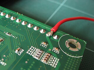
Soldering is a process of joining two metal surfaces together using a filler metal called solder. The soldering process involves heating the surfaces to be joined and melting the solder, which is then allowed to cool and solidify, creating a strong and durable joint.

Chip on board (COB) is a method of circuit board manufacturing in which the integrated circuits (e.g. microprocessors) are attached (wired, bonded directly) to a printed circuit board, and covered by a blob of epoxy. Chip on board eliminates the packaging of individual semiconductor devices, which allows a completed product to be less costly, lighter, and more compact. In some cases, COB construction improves the operation of radio frequency systems by reducing the inductance and capacitance of integrated circuit leads.