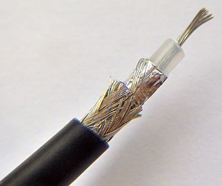
In electrical engineering, a transmission line is a specialized cable or other structure designed to conduct electromagnetic waves in a contained manner. The term applies when the conductors are long enough that the wave nature of the transmission must be taken into account. This applies especially to radio-frequency engineering because the short wavelengths mean that wave phenomena arise over very short distances. However, the theory of transmission lines was historically developed to explain phenomena on very long telegraph lines, especially submarine telegraph cables.

A DIMM, or Dual In-Line Memory Module, is a type of computer memory module used in desktop, laptop, and server computers. It is a circuit board that contains memory chips and connects to the computer's motherboard. A DIMM is often called a "RAM stick" due to its shape and size. A DIMM comprises a series of dynamic random-access memory integrated circuits that are mounted to its circuit board. DIMMs are the predominant method for adding memory into a computer system. The vast majority of DIMMs are standardized through JEDEC standards, although there are proprietary DIMMs. DIMMs come in a variety of speeds and sizes, but generally are one of two lengths - PC which are 133.35 mm (5.25 in) and laptop (SO-DIMM) which are about half the size at 67.60 mm (2.66 in).
Rambus DRAM (RDRAM), and its successors Concurrent Rambus DRAM (CRDRAM) and Direct Rambus DRAM (DRDRAM), are types of synchronous dynamic random-access memory (SDRAM) developed by Rambus from the 1990s through to the early 2000s. The third-generation of Rambus DRAM, DRDRAM was replaced by XDR DRAM. Rambus DRAM was developed for high-bandwidth applications and was positioned by Rambus as replacement for various types of contemporary memories, such as SDRAM.

In electrical engineering, impedance matching is the practice of designing or adjusting the input impedance or output impedance of an electrical device for a desired value. Often, the desired value is selected to maximize power transfer or minimize signal reflection. For example, impedance matching typically is used to improve power transfer from a radio transmitter via the interconnecting transmission line to the antenna. Signals on a transmission line will be transmitted without reflections if the transmission line is terminated with a matching impedance.

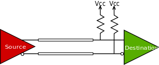
In electronics, electrical termination is the practice of ending a transmission line with a device that matches the characteristic impedance of the line. Termination prevents signals from reflecting off the end of the transmission line. Reflections at the ends of unterminated transmission lines cause distortion, which can produce ambiguous digital signal levels and misoperation of digital systems. Reflections in analog signal systems cause such effects as video ghosting, or power loss in radio transmitter transmission lines.
Rambus Inc. is an American technology company that designs, develops and licenses chip interface technologies and architectures that are used in digital electronics products. The company, founded in 1990, is well known for inventing RDRAM and for its intellectual property-based litigation following the introduction of DDR-SDRAM memory.
In electrical engineering, the input impedance of an electrical network is the measure of the opposition to current (impedance), both static (resistance) and dynamic (reactance), into a load network that is external to the electrical source network. The input admittance is a measure of the load network's propensity to draw current. The source network is the portion of the network that transmits power, and the load network is the portion of the network that consumes power.
RS-485, also known as TIA-485(-A) or EIA-485, is a standard, originally introduced in 1983, defining the electrical characteristics of drivers and receivers for use in serial communications systems. Electrical signaling is balanced, and multipoint systems are supported. The standard is jointly published by the Telecommunications Industry Association and Electronic Industries Alliance (TIA/EIA). Digital communications networks implementing the standard can be used effectively over long distances and in electrically noisy environments. Multiple receivers may be connected to such a network in a linear, multidrop bus. These characteristics make RS-485 useful in industrial control systems and similar applications.
MIL-STD-1553 is a military standard published by the United States Department of Defense that defines the mechanical, electrical, and functional characteristics of a serial data bus. It was originally designed as an avionic data bus for use with military avionics, but has also become commonly used in spacecraft on-board data handling (OBDH) subsystems, both military and civil, including use on the James Webb space telescope. It features multiple redundant balanced line physical layers, a (differential) network interface, time-division multiplexing, half-duplex command/response protocol, and can handle up to 31 Remote Terminals (devices); 32 is typically designated for broadcast messages. A version of MIL-STD-1553 using optical cabling in place of electrical is known as MIL-STD-1773.
Current mode logic (CML), or source-coupled logic (SCL), is a digital design style used both for logic gates and for board-level digital signaling of digital data.
XDR DRAM is a high-performance dynamic random-access memory interface. It is based on and succeeds RDRAM. Competing technologies include DDR2 and GDDR4.

Electronic filters are a type of signal processing filter in the form of electrical circuits. This article covers those filters consisting of lumped electronic components, as opposed to distributed-element filters. That is, using components and interconnections that, in analysis, can be considered to exist at a single point. These components can be in discrete packages or part of an integrated circuit.

Microstrip is a type of electrical transmission line which can be fabricated with any technology where a conductor is separated from a ground plane by a dielectric layer known as "substrate". Microstrip lines are used to convey microwave-frequency signals.

Signal integrity or SI is a set of measures of the quality of an electrical signal. In digital electronics, a stream of binary values is represented by a voltage waveform. However, digital signals are fundamentally analog in nature, and all signals are subject to effects such as noise, distortion, and loss. Over short distances and at low bit rates, a simple conductor can transmit this with sufficient fidelity. At high bit rates and over longer distances or through various mediums, various effects can degrade the electrical signal to the point where errors occur and the system or device fails. Signal integrity engineering is the task of analyzing and mitigating these effects. It is an important activity at all levels of electronics packaging and assembly, from internal connections of an integrated circuit (IC), through the package, the printed circuit board (PCB), the backplane, and inter-system connections. While there are some common themes at these various levels, there are also practical considerations, in particular the interconnect flight time versus the bit period, that cause substantial differences in the approach to signal integrity for on-chip connections versus chip-to-chip connections.
In computing, a memory module or RAM stick is a printed circuit board on which memory integrated circuits are mounted. Memory modules permit easy installation and replacement in electronic systems, especially computers such as personal computers, workstations, and servers. The first memory modules were proprietary designs that were specific to a model of computer from a specific manufacturer. Later, memory modules were standardized by organizations such as JEDEC and could be used in any system designed to use them.
An electronic circuit is composed of individual electronic components, such as resistors, transistors, capacitors, inductors and diodes, connected by conductive wires or traces through which electric current can flow. It is a type of electrical circuit. For a circuit to be referred to as electronic, rather than electrical, generally at least one active component must be present. The combination of components and wires allows various simple and complex operations to be performed: signals can be amplified, computations can be performed, and data can be moved from one place to another.

Zobel networks are a type of filter section based on the image-impedance design principle. They are named after Otto Zobel of Bell Labs, who published a much-referenced paper on image filters in 1923. The distinguishing feature of Zobel networks is that the input impedance is fixed in the design independently of the transfer function. This characteristic is achieved at the expense of a much higher component count compared to other types of filter sections. The impedance would normally be specified to be constant and purely resistive. For this reason, Zobel networks are also known as constant resistance networks. However, any impedance achievable with discrete components is possible.

In electronics, signal processing, and video, ringing is oscillation of a signal, particularly in the step response. Often ringing is undesirable, but not always, as in the case of resonant inductive coupling. It is also known as hunting.
A distributed-element filter is an electronic filter in which capacitance, inductance, and resistance are not localised in discrete capacitors, inductors, and resistors as they are in conventional filters. Its purpose is to allow a range of signal frequencies to pass, but to block others. Conventional filters are constructed from inductors and capacitors, and the circuits so built are described by the lumped element model, which considers each element to be "lumped together" at one place. That model is conceptually simple, but it becomes increasingly unreliable as the frequency of the signal increases, or equivalently as the wavelength decreases. The distributed-element model applies at all frequencies, and is used in transmission-line theory; many distributed-element components are made of short lengths of transmission line. In the distributed view of circuits, the elements are distributed along the length of conductors and are inextricably mixed together. The filter design is usually concerned only with inductance and capacitance, but because of this mixing of elements they cannot be treated as separate "lumped" capacitors and inductors. There is no precise frequency above which distributed element filters must be used but they are especially associated with the microwave band.

Commensurate line circuits are electrical circuits composed of transmission lines that are all the same length; commonly one-eighth of a wavelength. Lumped element circuits can be directly converted to distributed-element circuits of this form by the use of Richards' transformation. This transformation has a particularly simple result; inductors are replaced with transmission lines terminated in short-circuits and capacitors are replaced with lines terminated in open-circuits. Commensurate line theory is particularly useful for designing distributed-element filters for use at microwave frequencies.