R4000

Last updated
A Toshiba R4000 microprocessor KL Toshiba MIPS R4000.jpg
A Toshiba R4000 microprocessor
MIPS R4000 die shot MIPS R4000 die.JPG
MIPS R4000 die shot

The R4000 is a microprocessor developed by MIPS Computer Systems that implements the MIPS III instruction set architecture (ISA). Officially announced on 1 October 1991, it was one of the first 64-bit microprocessors and the first MIPS III implementation. In the early 1990s, when RISC microprocessors were expected to replace CISC microprocessors such as the Intel i486, the R4000 was selected to be the microprocessor of the Advanced Computing Environment (ACE), an industry standard that intended to define a common RISC platform. ACE ultimately failed for a number of reasons, but the R4000 found success in the workstation and server markets.

Contents

Models

There are three configurations of the R4000: the R4000PC, an entry-level model with no support for a secondary cache; the R4000SC, a model with secondary cache but no multiprocessor capability; and the R4000MC, a model with secondary cache and support for the cache coherency protocols required by multiprocessor systems.

Description

The R4000 is a scalar superpipelined microprocessor with an eight-stage integer pipeline. During the first stage (IF), a virtual address for an instruction is generated and the instruction translation lookaside buffer (TLB) begins the translation of the address to a physical address. In the second stage (IS), translation is completed and the instruction is fetched from an internal 8 KB instruction cache. The instruction cache is direct-mapped and virtually indexed, physically tagged. It has a 16- or 32-byte line size. Architecturally, it could be expanded to 32 KB.

During the third stage (RF), the instruction is decoded and the register file is read. The MIPS III defines two register files, one for the integer unit and the other for floating-point. Each register file is 64 bits wide and contained 32 entries. The integer register file has two read ports and one write port, while the floating-point register file has two read ports and two write ports. Execution begins at stage four (EX) for both integer and floating-point instructions; and is written back to the register files when completed in stage eight (WB). Results may be bypassed if possible.

Integer execution

The R4000 has an arithmetic logic unit (ALU), a shifter, multiplier and divider and load aligner for executing integer instructions. The ALU consists of a 64-bit carry-select adder and a logic unit and is pipelined. The shifter is a 32-bit barrel shifter. It performs 64-bit shifts in two cycles, stalling the pipeline as a result. This design was chosen to save die area. The multiplier and divider are not pipelined and have significant latencies: multiplies have a 10- or 20-cycle latency for 32-bit or 64-bit integers, respectively; whereas divides have a 69- or 133-cycle latency for 32-bit or 64-bit integers, respectively. Most instructions have a single cycle latency. The ALU adder is also used for calculating virtual addresses for loads, stores and branches.

Load and store instructions are executed by the integer pipeline, and access the on-chip 8 KB data cache.

Floating-point execution

The R4000 has an on-die IEEE 754-1985-compliant floating-point unit (FPU), referred to as the R4010. The FPU is a coprocessor designated CP1 [1] (the MIPS ISA defined four coprocessors, designated CP0 to CP3). The FPU can operate in two modes, 32- or 64-bit which are selected by setting a bit, the FR bit, in the CPU status register. In 32-bit mode, the 32 floating-point registers become 32 bits wide when used to hold single-precision floating-point numbers. When used to hold double-precision numbers, there are 16 floating-point registers (the registers are paired).

The FPU can operate in parallel with the ALU unless there is a data or resource dependency, which causes it to stall. It contains three sub-units: an adder, a multiplier and a divider. The multiplier and divider can execute an instruction in parallel with the adder, but they use the adder in their final stages of execution, thus imposing limits to overlapping execution. Thus, under certain conditions, it can execute up to three instructions at any time, one in each unit. The FPU is capable of retiring one instruction per cycle.

The adder and multiplier are pipelined. The multiplier has a four-stage multiplier pipeline. It is clocked at twice the clock frequency of the microprocessor for adequate performance and uses dynamic logic to achieve the high clock frequency. Division has a 23- or 36-cycle latency for single- or double-precision operations and square-root has a 54- or 112-cycle latency. Division and square-root uses the SRT algorithm.

Memory management

The memory management unit (MMU) uses a 48-entry translation lookaside buffer to translate virtual addresses. The R4000 uses a 64-bit virtual address, but only implements 40 of the 64 bits, allowing 1 TB of virtual memory; the remaining bits are checked to ensure that they contain zero. The R4000 uses a 36-bit physical address, thus is able to address 64 GB of physical memory.

Secondary cache

The R4000 (SC and MC configurations only) supports an external secondary cache with a capacity of 128 KB to 4 MB. The cache is accessed via a dedicated 128-bit data bus. The secondary cache can be configured either as a unified cache or as a split instruction and data cache. In the latter configuration, each cache can have a capacity of 128 KB to 2 MB. [2] The secondary cache is physically indexed, physically tagged and has a programmable line size of 128, 256, 512 or 1,024 bytes. The cache controller is on-die. The cache is built from standard static random access memory (SRAM). The data and tag buses are ECC-protected.

System bus

The R4000 uses a 64-bit system bus called the SysAD bus. The SysAD bus was an address and data multiplexed bus, that is, it used the same set of wires to transfer data and addresses. While this reduces bandwidth, it is also less expensive than providing a separate address bus, which requires more pins and increases the complexity of the system. The SysAD bus can be configured to operate at half, a third or a quarter of the internal clock frequency. The SysAD bus generates its clock signal by dividing the operating frequency.

Transistor count, die dimensions and process details

The R4000 contains 1.2 million transistors. [3] It was designed for a 1.0 μm two-layer metal complementary metaloxidesemiconductor (CMOS) process. As MIPS was a fabless company, the R4000 was fabricated by partners in their own processes, which had a 0.8 μm minimum feature size. [4]

Clocking

The R4000 generates the various clock signals from a master clock signal generated externally. For the operating frequency, the R4000 multiplies the master clock signal by two by use of an on-die phase-locked loop (PLL).

Packaging

The R4000PC is packaged in a 179-pin ceramic pin grid array (CPGA). The R4000SC and R4000MC are packaged in a 447-pin ceramic staggered pin grid array (SPGA). The pin out of the R4000MC is different from the R4000SC, with some pins which are unused on the R4000SC used for signals to implement cache coherency on the R4000MC. The pin-out of the R4000PC is similar to that of the PGA-packaged R4200 and R4600 microprocessors. This characteristic enables a properly designed system to use any of the three microprocessors.

R4400

An example of a R4400MC microprocessor fabricated by Toshiba Toshiba TC86R4400MC-200 9636YJA top.jpg
An example of a R4400MC microprocessor fabricated by Toshiba
NEC VR4400MC die shot NEC VR4400 die.JPG
NEC VR4400MC die shot

The R4400 is a further development of the R4000. It was announced in early November 1992. Samples of the microprocessor had been shipped to selected customers before then, with general availability in January 1993. The R4400 operates at clock frequencies of 100, 133, 150, 200, and 250 MHz. The only major improvement from the R4000 is larger primary caches, which were doubled in capacity to 16 KB each from 8 KB each. It contained 2.3 million transistors.

The R4400 was licensed by Integrated Device Technology (IDT), LSI Logic, NEC, Performance Semiconductor, Siemens AG and Toshiba. IDT, NEC, Siemens and Toshiba fabricated and marketed the microprocessor. LSI Logic used the R4400 in custom products. Performance Semiconductor sold their logic division to Cypress Semiconductor where the MIPS microprocessor products were discontinued.

NEC marketed their version as the VR4400. The first version, a 150 MHz part, was announced in November 1992. Early versions were fabricated in a 0.6 μm process. [5] In mid-1995, a 250 MHz part began sampling. It was fabricated in a 0.35 μm four-layer-metal process. [6] NEC also produced the MR4401, a ceramic multi-chip module (MCM) that contained a VR4400SC with ten 1 Mbit SRAM chips that implemented a 1 MB secondary cache. The MCM was pin-compatible with the R4x00PC. The first version, a 150 MHz part, was announced in 1994. In 1995, a 200 MHz part was announced.

Toshiba marketed their version as the TC86R4400. A 200 MHz part containing 2.3 million transistors and measuring 134 mm2 fabricated in a 0.3 μm process was introduced in mid-1994. The R4400PC was priced at $1,600, the R4400SC at $1,950, and the R4400MC at $2,150 in quantities of 10,000. [7]

Usage

The R4400 is used by:

Chipsets

The R4000 and R4400 microprocessors were interfaced to the system by custom ASICs or by commercially available chipsets. System vendors such as SGI developed their own ASICs for their systems. Commercial chipsets were developed, fabricated and marketed by companies such as Toshiba with their the Tiger Shark chipset, which provided a i486-compatible bus. [13]

Notes

  1. MIPS R4000 Microprocessor User's Manual, Second Edition, p. 152
  2. Heinrich, "MIPS R4000 Microprocessor User's Manual", p. 248
  3. Mirapuri, "The Mips R4000 Processor", p. 10
  4. Mirapuri, "The Mips R4000 Processor", p. 21
  5. "NEC VR4400 Clock-Doubling RISC Has 2m Transistors"
  6. "NEC Ready With 250MHz Version Of The 64-Bit MIPS R4400 RISC"
  7. "Toshiba Has 200MHz MIPS R4400"
  8. "...And From Carrera Computers"
  9. "Concurrent Multiprocessors Feature New Bus Architecture"
  10. "MIPS R-Based Windows NT Personal Computers From Deskstation..."
  11. "NEC Goes After The Business Market With Its Latest Line Of RISC UNIX Workstations"
  12. "Pyramid Technology Aims To Crash The Mainframe With Nile Series"
  13. "Toshiba Samples 80486-Bus Chip Set For R-Series".

Related Research Articles

MIPS is a family of reduced instruction set computer (RISC) instruction set architectures (ISA) developed by MIPS Computer Systems, now MIPS Technologies, based in the United States.

The Intel i860 is a RISC microprocessor design introduced by Intel in 1989. It is one of Intel's first attempts at an entirely new, high-end instruction set architecture since the failed Intel iAPX 432 from the beginning of the 1980s. It was the world's first million-transistor chip. It was released with considerable fanfare, slightly obscuring the earlier Intel i960, which was successful in some niches of embedded systems. The i860 never achieved commercial success and the project was terminated in the mid-1990s.

<span class="mw-page-title-main">Pentium Pro</span> Sixth-generation x86 microprocessor by Intel

The Pentium Pro is a sixth-generation x86 microprocessor developed and manufactured by Intel and introduced on November 1, 1995. It introduced the P6 microarchitecture and was originally intended to replace the original Pentium in a full range of applications. While the Pentium and Pentium MMX had 3.1 and 4.5 million transistors, respectively, the Pentium Pro contained 5.5 million transistors. Later, it was reduced to a more narrow role as a server and high-end desktop processor and was used in supercomputers like ASCI Red, the first computer to reach the trillion floating point operations per second (teraFLOPS) performance mark. The Pentium Pro was capable of both dual- and quad-processor configurations. It only came in one form factor, the relatively large rectangular Socket 8. The Pentium Pro was succeeded by the Pentium II Xeon in 1998.

<span class="mw-page-title-main">Quantum Effect Devices</span> Microprocessor design company

Quantum Effect Devices (QED) was a microprocessor design company incorporated in 1991 as Quantum Effect Design. It was based in Palo Alto, California.

<span class="mw-page-title-main">Emotion Engine</span>

The Emotion Engine is a central processing unit developed and manufactured by Sony Computer Entertainment and Toshiba for use in the PlayStation 2 video game console. It was also used in early PlayStation 3 models sold in Japan and North America to provide PlayStation 2 game support. Mass production of the Emotion Engine began in 1999 and ended in late 2012 with the discontinuation of the PlayStation 2.

SPARC64 is a microprocessor developed by HAL Computer Systems and fabricated by Fujitsu. It implements the SPARC V9 instruction set architecture (ISA), the first microprocessor to do so. SPARC64 was HAL's first microprocessor and was the first in the SPARC64 brand. It operates at 101 and 118 MHz. The SPARC64 was used exclusively by Fujitsu in their systems; the first systems, the Fujitsu HALstation Model 330 and Model 350 workstations, were formally announced in September 1995 and were introduced in October 1995, two years late. It was succeeded by the SPARC64 II in 1996.

<span class="mw-page-title-main">AMD Am29000</span>

The AMD Am29000, commonly shortened to 29k, is a family of 32-bit RISC microprocessors and microcontrollers developed and fabricated by Advanced Micro Devices (AMD). Based on the seminal Berkeley RISC, the 29k added a number of significant improvements. They were, for a time, the most popular RISC chips on the market, widely used in laser printers from a variety of manufacturers.

<span class="mw-page-title-main">POWER3</span> 1998 family of microprocessors by IBM

The POWER3 is a microprocessor, designed and exclusively manufactured by IBM, that implemented the 64-bit version of the PowerPC instruction set architecture (ISA), including all of the optional instructions of the ISA such as instructions present in the POWER2 version of the POWER ISA but not in the PowerPC ISA. It was introduced on 5 October 1998, debuting in the RS/6000 43P Model 260, a high-end graphics workstation. The POWER3 was originally supposed to be called the PowerPC 630 but was renamed, probably to differentiate the server-oriented POWER processors it replaced from the more consumer-oriented 32-bit PowerPCs. The POWER3 was the successor of the P2SC derivative of the POWER2 and completed IBM's long-delayed transition from POWER to PowerPC, which was originally scheduled to conclude in 1995. The POWER3 was used in IBM RS/6000 servers and workstations at 200 MHz. It competed with the Digital Equipment Corporation (DEC) Alpha 21264 and the Hewlett-Packard (HP) PA-8500.

<span class="mw-page-title-main">R10000</span> MIPS microprocessor

The R10000, code-named "T5", is a RISC microprocessor implementation of the MIPS IV instruction set architecture (ISA) developed by MIPS Technologies, Inc. (MTI), then a division of Silicon Graphics, Inc. (SGI). The chief designers are Chris Rowen and Kenneth C. Yeager. The R10000 microarchitecture is known as ANDES, an abbreviation for Architecture with Non-sequential Dynamic Execution Scheduling. The R10000 largely replaces the R8000 in the high-end and the R4400 elsewhere. MTI was a fabless semiconductor company; the R10000 was fabricated by NEC and Toshiba. Previous fabricators of MIPS microprocessors such as Integrated Device Technology (IDT) and three others did not fabricate the R10000 as it was more expensive to do so than the R4000 and R4400.

<span class="mw-page-title-main">R3000</span> RISC microprocessor

The R3000 is a 32-bit RISC microprocessor chipset developed by MIPS Computer Systems that implemented the MIPS I instruction set architecture (ISA). Introduced in June 1988, it was the second MIPS implementation, succeeding the R2000 as the flagship MIPS microprocessor. It operated at 20, 25 and 33.33 MHz.

<span class="mw-page-title-main">R5000</span>

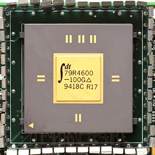
The R5000 is a 64-bit, bi-endian, superscalar, in-order execution 2-issue design microprocessor, that implements the MIPS IV instruction set architecture (ISA) developed by Quantum Effect Design (QED) in 1996. The project was funded by MIPS Technologies, Inc (MTI), also the licensor. MTI then licensed the design to Integrated Device Technology (IDT), NEC, NKK, and Toshiba. The R5000 succeeded the QED R4600 and R4700 as their flagship high-end embedded microprocessor. IDT marketed its version of the R5000 as the 79RV5000, NEC as VR5000, NKK as the NR5000, and Toshiba as the TX5000. The R5000 was sold to PMC-Sierra when the company acquired QED. Derivatives of the R5000 are still in production today for embedded systems.

The R8000 is a microprocessor chipset developed by MIPS Technologies, Inc. (MTI), Toshiba, and Weitek. It was the first implementation of the MIPS IV instruction set architecture. The R8000 is also known as the TFP, for Tremendous Floating-Point, its name during development.

<span class="mw-page-title-main">Alpha 21064</span>

The Alpha 21064 is a microprocessor developed and fabricated by Digital Equipment Corporation that implemented the Alpha instruction set architecture (ISA). It was introduced as the DECchip 21064 before it was renamed in 1994. The 21064 is also known by its code name, EV4. It was announced in February 1992 with volume availability in September 1992. The 21064 was the first commercial implementation of the Alpha ISA, and the first microprocessor from Digital to be available commercially. It was succeeded by a derivative, the Alpha 21064A in October 1993. This last version was replaced by the Alpha 21164 in 1995.

<span class="mw-page-title-main">Alpha 21164</span>

The Alpha 21164, also known by its code name, EV5, is a microprocessor developed and fabricated by Digital Equipment Corporation that implemented the Alpha instruction set architecture (ISA). It was introduced in January 1995, succeeding the Alpha 21064A as Digital's flagship microprocessor. It was succeeded by the Alpha 21264 in 1998.

<span class="mw-page-title-main">Alpha 21264</span>

The Alpha 21264 is a Digital Equipment Corporation RISC microprocessor launched on 19 October 1998. The 21264 implemented the Alpha instruction set architecture (ISA).

<span class="mw-page-title-main">PA-8000</span>

The PA-8000 (PCX-U), code-named Onyx, is a microprocessor developed and fabricated by Hewlett-Packard (HP) that implemented the PA-RISC 2.0 instruction set architecture (ISA). It was a completely new design with no circuitry derived from previous PA-RISC microprocessors. The PA-8000 was introduced on 2 November 1995 when shipments began to members of the Precision RISC Organization (PRO). It was used exclusively by PRO members and was not sold on the merchant market. All follow-on PA-8x00 processors are based on the basic PA-8000 processor core.

<span class="mw-page-title-main">TurboSPARC</span>

The TurboSPARC is a microprocessor that implements the SPARC V8 instruction set architecture (ISA) developed by Fujitsu Microelectronics, Inc. (FMI), the United States subsidiary of the Japanese multinational information technology equipment and services company Fujitsu Limited located in San Jose, California. It was a low-end microprocessor primarily developed as an upgrade for the Sun Microsystems microSPARC-II-based SPARCstation 5 workstation. It was introduced on 30 September 1996, with a 170 MHz version priced at US$499 in quantities of 1,000. The TurboSPARC was mostly succeeded in the low-end SPARC market by the UltraSPARC IIi in late 1997, but remained available.

The R4200 is a microprocessor designed by MIPS Technologies, Inc. (MTI) that implemented the MIPS III instruction set architecture (ISA). It was also known as the VRX during development. The microprocessor was licensed to NEC, and the company fabricated and marketed it as the VR4200. The first VR4200, an 80 MHz part, was introduced in 1993. A faster 100 MHz part became available in 1994.

<span class="mw-page-title-main">R4600</span>

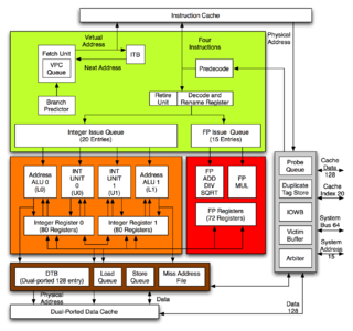
The R4600, code-named "Orion", is a microprocessor developed by Quantum Effect Design (QED) that implemented the MIPS III instruction set architecture (ISA). As QED was a design firm that did not fabricate or sell their designs, the R4600 was first licensed to Integrated Device Technology (IDT), and later to Toshiba and then NKK. These companies fabricated the microprocessor and marketed it. The R4600 was designed as a low-end workstation or high-end embedded microprocessor. Users included Silicon Graphics, Inc. (SGI) for their Indy workstation and DeskStation Technology for their Windows NT workstations. The R4600 was instrumental in making the Indy successful by providing good integer performance at a competitive price. In embedded systems, prominent users included Cisco Systems in their network routers and Canon in their printers.

Since 1985, many processors implementing some version of the MIPS architecture have been designed and used widely.

References