
MEMS is the technology of microscopic devices incorporating both electronic and moving parts. MEMS are made up of components between 1 and 100 micrometres in size, and MEMS devices generally range in size from 20 micrometres to a millimetre, although components arranged in arrays can be more than 1000 mm2. They usually consist of a central unit that processes data and several components that interact with the surroundings.
Photolithography is a process used in the manufacturing of integrated circuits. It involves using light to transfer a pattern onto a substrate, typically a silicon wafer.

A photoresist is a light-sensitive material used in several processes, such as photolithography and photoengraving, to form a patterned coating on a surface. This process is crucial in the electronics industry.

A photomask is an opaque plate with transparent areas that allow light to shine through in a defined pattern. Photomasks are commonly used in photolithography for the production of integrated circuits to produce a pattern on a thin wafer of material. In semiconductor manufacturing, a mask is sometimes called a reticle.
Since the mid-20th century, electron-beam technology has provided the basis for a variety of novel and specialized applications in semiconductor manufacturing, microelectromechanical systems, nanoelectromechanical systems, and microscopy.
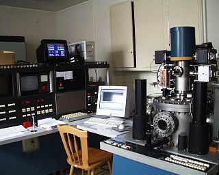
Electron-beam lithography is the practice of scanning a focused beam of electrons to draw custom shapes on a surface covered with an electron-sensitive film called a resist (exposing). The electron beam changes the solubility of the resist, enabling selective removal of either the exposed or non-exposed regions of the resist by immersing it in a solvent (developing). The purpose, as with photolithography, is to create very small structures in the resist that can subsequently be transferred to the substrate material, often by etching.
Masklesslithography (MPL) is a photomask-less photolithography-like technology used to project or focal-spot write the image pattern onto a chemical resist-coated substrate by means of UV radiation or electron beam.
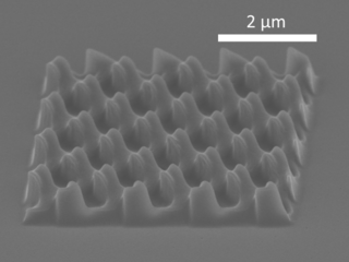
Nanolithography (NL) is a growing field of techniques within nanotechnology dealing with the engineering of nanometer-scale structures on various materials.
Next-generation lithography or NGL is a term used in integrated circuit manufacturing to describe the lithography technologies in development which are intended to replace current techniques. Driven by Moore's law in the semiconductor industries, the shrinking of the chip size and critical dimension continues. The term applies to any lithography method which uses a shorter-wavelength light or beam type than the current state of the art, such as X-ray lithography, electron beam lithography, focused ion beam lithography, and nanoimprint lithography. The term may also be used to describe techniques which achieve finer resolution features from an existing light wavelength.

Dip pen nanolithography (DPN) is a scanning probe lithography technique where an atomic force microscope (AFM) tip is used to create patterns directly on a range of substances with a variety of inks. A common example of this technique is exemplified by the use of alkane thiolates to imprint onto a gold surface. This technique allows surface patterning on scales of under 100 nanometers. DPN is the nanotechnology analog of the dip pen, where the tip of an atomic force microscope cantilever acts as a "pen", which is coated with a chemical compound or mixture acting as an "ink", and put in contact with a substrate, the "paper".
Nanoimprint lithography (NIL) is a method of fabricating nanometer-scale patterns. It is a simple nanolithography process with low cost, high throughput and high resolution. It creates patterns by mechanical deformation of imprint resist and subsequent processes. The imprint resist is typically a monomer or polymer formulation that is cured by heat or UV light during the imprinting. Adhesion between the resist and the template is controlled to allow proper release.
Contact lithography, also known as contact printing, is a form of photolithography whereby the image to be printed is obtained by illumination of a photomask in direct contact with a substrate coated with an imaging photoresist layer.

LIGA is a fabrication technology used to create high-aspect-ratio microstructures. The term is a German acronym for Lithographie, Galvanoformung, Abformung – lithography, electroplating, and molding.
Patterned media is a potential future hard disk drive technology to record data in magnetic islands, as opposed to current hard disk drive technology where each bit is stored in 20–30 magnetic grains within a continuous magnetic film. The islands would be patterned from a precursor magnetic film using nanolithography. It is one of the proposed technologies to succeed perpendicular recording due to the greater storage densities it would enable. BPM was introduced by Toshiba in 2010.
The lift-off process in microstructuring technology is a method of creating structures (patterning) of a target material on the surface of a substrate using a sacrificial material . It is an additive technique as opposed to more traditional subtracting technique like etching. The scale of the structures can vary from the nanoscale up to the centimeter scale or further, but are typically of micrometric dimensions.
Plasmonic nanolithography is a nanolithographic process that utilizes surface plasmon excitations such as surface plasmon polaritons (SPPs) to fabricate nanoscale structures. SPPs, which are surface waves that propagate in between planar dielectric-metal layers in the optical regime, can bypass the diffraction limit on the optical resolution that acts as a bottleneck for conventional photolithography.
Stencil lithography is a novel method of fabricating nanometer scale patterns using nanostencils, stencils with nanometer size apertures. It is a resist-less, simple, parallel nanolithography process, and it does not involve any heat or chemical treatment of the substrates .

X-ray lithography is a process used in semiconductor device fabrication industry to selectively remove parts of a thin film of photoresist. It uses X-rays to transfer a geometric pattern from a mask to a light-sensitive chemical photoresist, or simply "resist," on the substrate to reach extremely small topological size of a feature. A series of chemical treatments then engraves the produced pattern into the material underneath the photoresist.
Three-dimensional (3D) microfabrication refers to manufacturing techniques that involve the layering of materials to produce a three-dimensional structure at a microscopic scale. These structures are usually on the scale of micrometers and are popular in microelectronics and microelectromechanical systems.
Glossary of microelectronics manufacturing terms