Chemical vapor deposition (CVD) is a vacuum deposition method used to produce high-quality, and high-performance, solid materials. The process is often used in the semiconductor industry to produce thin films.
Photolithography is a process used in the manufacturing of integrated circuits. It involves using light to transfer a pattern onto a substrate, typically a silicon wafer.

A photoresist is a light-sensitive material used in several processes, such as photolithography and photoengraving, to form a patterned coating on a surface. This process is crucial in the electronics industry.
A thin film is a layer of material ranging from fractions of a nanometer (monolayer) to several micrometers in thickness. The controlled synthesis of materials as thin films is a fundamental step in many applications. A familiar example is the household mirror, which typically has a thin metal coating on the back of a sheet of glass to form a reflective interface. The process of silvering was once commonly used to produce mirrors, while more recently the metal layer is deposited using techniques such as sputtering. Advances in thin film deposition techniques during the 20th century have enabled a wide range of technological breakthroughs in areas such as magnetic recording media, electronic semiconductor devices, integrated passive devices, LEDs, optical coatings, hard coatings on cutting tools, and for both energy generation and storage. It is also being applied to pharmaceuticals, via thin-film drug delivery. A stack of thin films is called a multilayer.
A coating is a covering that is applied to the surface of an object, usually referred to as the substrate. The purpose of applying the coating may be decorative, functional, or both. Coatings may be applied as liquids, gases or solids e.g. Powder coatings.
Nanoimprint lithography (NIL) is a method of fabricating nanometer-scale patterns. It is a simple nanolithography process with low cost, high throughput and high resolution. It creates patterns by mechanical deformation of imprint resist and subsequent processes. The imprint resist is typically a monomer or polymer formulation that is cured by heat or UV light during the imprinting. Adhesion between the resist and the template is controlled to allow proper release.

Compact disc manufacturing is the process by which commercial compact discs (CDs) are replicated in mass quantities using a master version created from a source recording. This may be either in audio form (CD-DA) or data form (CD-ROM). This process is used in the mastering of read-only compact discs. DVDs and Blu-rays use similar methods.
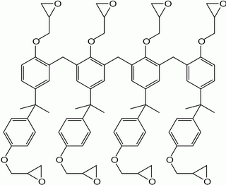
SU-8 is a commonly used epoxy-based negative photoresist. Negative refers to a photoresist whereby the parts exposed to UV become cross-linked, while the remainder of the film remains soluble and can be washed away during development.

Dip coating is an industrial coating process which is used, for example, to manufacture bulk products such as coated fabrics and condoms and specialised coatings for example in the biomedical field. Dip coating is also commonly used in academic research, where many chemical and nano material engineering research projects use the dip coating technique to create thin-film coatings.
Physical vapor deposition (PVD), sometimes called physical vapor transport (PVT), describes a variety of vacuum deposition methods which can be used to produce thin films and coatings on substrates including metals, ceramics, glass, and polymers. PVD is characterized by a process in which the material transitions from a condensed phase to a vapor phase and then back to a thin film condensed phase. The most common PVD processes are sputtering and evaporation. PVD is used in the manufacturing of items which require thin films for optical, mechanical, electrical, acoustic or chemical functions. Examples include semiconductor devices such as thin-film solar cells, microelectromechanical devices such as thin film bulk acoustic resonator, aluminized PET film for food packaging and balloons, and titanium nitride coated cutting tools for metalworking. Besides PVD tools for fabrication, special smaller tools used mainly for scientific purposes have been developed.

Evaporation is a common method of thin-film deposition. The source material is evaporated in a vacuum. The vacuum allows vapor particles to travel directly to the target object (substrate), where they condense back to a solid state. Evaporation is used in microfabrication, and to make macro-scale products such as metallized plastic film.
An electrochromic device (ECD) controls optical properties such as optical transmission, absorption, reflectance and/or emittance in a continual but reversible manner on application of voltage (electrochromism). This property enables an ECD to be used for applications like smart glass, electrochromic mirrors, and electrochromic display devices.

Ultrasonic nozzles are a type of spray nozzle that use high frequency vibrations produced by piezoelectric transducers acting upon the nozzle tip that create capillary waves in a liquid film. Once the amplitude of the capillary waves reaches a critical height, they become too tall to support themselves and tiny droplets fall off the tip of each wave resulting in atomization.
Curtain coating is a process that creates an uninterrupted curtain of fluid that falls onto a substrate. The substrate is transported on a conveyor belt or calender rolls at a regulated speed through the curtain to ensure an even coat of the die. The curtain is created by using a slit or die at the base of the holding tank, allowing the liquid to fall upon the substrate. Some polymers are melted and extruded for coating. Many manufactures will also include a catch pan to retrieve and reuse the excess fluid.
Nanoarchitectures for lithium-ion batteries are attempts to employ nanotechnology to improve the design of lithium-ion batteries. Research in lithium-ion batteries focuses on improving energy density, power density, safety, durability and cost.
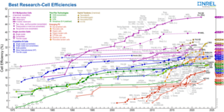
There are currently many research groups active in the field of photovoltaics in universities and research institutions around the world. This research can be categorized into three areas: making current technology solar cells cheaper and/or more efficient to effectively compete with other energy sources; developing new technologies based on new solar cell architectural designs; and developing new materials to serve as more efficient energy converters from light energy into electric current or light absorbers and charge carriers.

Photolithography is a process in removing select portions of thin films used in microfabrication. Microfabrication is the production of parts on the micro- and nano- scale, typically on the surface of silicon wafers, for the production of integrated circuits, microelectromechanical systems (MEMS), solar cells, and other devices. Photolithography makes this process possible through the combined use of hexamethyldisilazane (HMDS), photoresist, spin coating, photomask, an exposure system and other various chemicals. By carefully manipulating these factors it is possible to create nearly any geometry microstructure on the surface of a silicon wafer. The chemical interaction between all the different components and the surface of the silicon wafer makes photolithography an interesting chemistry problem. Current engineering has been able to create features on the surface of silicon wafers between 1 and 100 μm.
A. R. Forouhi and I. Bloomer deduced dispersion equations for the refractive index, n, and extinction coefficient, k, which were published in 1986 and 1988. The 1986 publication relates to amorphous materials, while the 1988 publication relates to crystalline. Subsequently, in 1991, their work was included as a chapter in “The Handbook of Optical Constants”. The Forouhi–Bloomer dispersion equations describe how photons of varying energies interact with thin films. When used with a spectroscopic reflectometry tool, the Forouhi–Bloomer dispersion equations specify n and k for amorphous and crystalline materials as a function of photon energy E. Values of n and k as a function of photon energy, E, are referred to as the spectra of n and k, which can also be expressed as functions of the wavelength of light, λ, since E = HC/λ. The symbol h represents Planck’s constant and c, the speed of light in vacuum. Together, n and k are often referred to as the “optical constants” of a material.
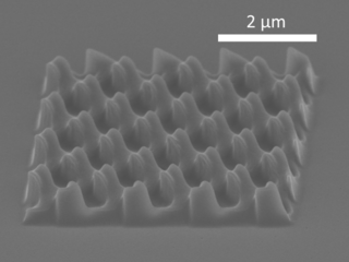
Three-dimensional (3D) microfabrication refers to manufacturing techniques that involve the layering of materials to produce a three-dimensional structure at a microscopic scale. These structures are usually on the scale of micrometers and are popular in microelectronics and microelectromechanical systems.

Slot-die coating is a coating technique for the application of solution, slurry, or extruded thin films onto typically flat substrates such as glass, metal, paper, fabric or plastic foils. The process was first developed for the industrial production of photographic papers in the 1950's. It has since become relevant in numerous commercial processes and nanomaterials related research fields.