Resonant-cavity-enhanced photo detector

Last updated

Resonant-cavity-enhanced photodetectors, also known as RCE photodetectors, are sensors designed to detect light or other forms of electromagnetic radiation. They achieve this by employing an optical cavity, a configuration of mirrors or other optical elements that forms a cavity resonator for light waves, allowing more efficient targeting of specific wavelengths.

Contents

With RCE photodetectors, the active device structure of a photodetector is placed inside a Fabry–Pérot interferometer. The interferometer has two parallel surfaces between which a selected wavelength of light can be made to resonate, amplifying the optical field. Though the active device structure of RCE detectors remains close to that of conventional photodetectors, the amplification effect of the optical cavity allows RCE photodetectors to be made thinner and therefore faster, while simultaneously increasing the quantum efficiency at the resonant wavelengths.

Advantages

The quantum efficiency of conventional detectors is dominated by the optical absorption (electromagnetic radiation) of the semiconductor material. For semiconductors with low absorption coefficients, a thicker absorption region is required to achieve adequate quantum efficiency, but at the cost of the signal-processing bandwidth of the photodetector.

An RCE detector can have significantly higher bandwidth than a conventional detector. The constructive interference of a Fabry–Pérot cavity enhances the optical field inside the photodetector at the resonance wavelengths to achieve a quantum efficiency of close to unity. Moreover, the optical cavity makes the RCE detectors wavelength selective, making RCE photodetectors attractive for low crosstalk wavelength demultiplexing.[ jargon ] Improved quantum efficiency reduces power consumption, while higher bandwidth translates to faster operation.

The RCE photodetectors have both wavelength selectivity and high-speed response making them ideal for wavelength division multiplexing applications. Optical modulators situated in an optical cavity require fewer quantum wells to absorb the same fraction of the incident light and can therefore operate at lower voltages. In the case of emitters, the cavity modifies the spontaneous emission of light-emitting diodes (LED) improving their spectral purity and directivity.

Thus, optical communication systems can perform much faster, with more bandwidth and can become more reliable. Camera sensors could give more resolutions, better contrast ratios and less distortion. For these reasons, RCE devices can be expected to play a growing role in optical electronics over the coming years.[ citation needed ]

Theory of RCE photo detectors

Compared to a conventional photodiode, RCE photo detectors can provide higher quantum efficiency, a higher detection speed and can also provide wavelength selective detection.

Quantum efficiency of RCE photo detectors

The RCE photodetectors are expected to have higher quantum efficiency η than compared to conventional photodiodes. The formulation of η for RCE devices gives insight to the design criteria.

A generalized RCE photodetector schematic as given in Figure 1 can give the required theoretical model of photodetection. A thin absorption region of thickness d is sandwiched between two relatively less absorbing region, substrate, of thickness L1 and L2. The optical cavity is formed by a period of λ/4 distributed Bragg reflector (DBR), made of non-absorbing larger bandgap materials, at the end of the substrate. The front mirror has a transmittance of t1 and generally has lower reflectivity than compared to the mirror at back (R1 < R2 ). Transmittance t1 allows light to enter into the cavity, and reflectivity R1 (=r12) and R2 (=r22) provides the optical confinement in the cavity.

The active region and the substrate region have absorption coefficient α and αex respectively. The field reflection coefficients of the front and the back mirrors are and respectively, where ф1 and ф2 are the phase shifts due to the light penetration (see Penetration Depth) into the mirrors.

The optical microcavity allows building up an optical field inside the optical cavity. In compared to conventional detector, where light is absorbed in a single pass through the absorption region, for RCE detectors trapped light is absorbed each time it traverses through the absorption region.

The Quantum efficiency for a RCE detector is given by:

Here . In practical detector design αex << α, so αex can be neglected and can be given as:

The term inside the [] represents the cavity enhancement effect. This is a periodic function of , which has minima at . And η enhanced periodically at resonance wavelength that meets this condition. The spacing of the resonant wavelength is given by the Free Spectral Range of the cavity.

The peak value of η at resonant wavelength is given as:

for a thin active layer as αd<<1, η becomes:

This is a significant improvement from the quantum efficiency of a conventional photodetector which is given by:

.

This shows that higher quantum efficiency can be achieved for smaller absorption regions.

The critical design requirements are a very high back mirror reflectivity and a moderate absorption layer thickness. At optical frequencies, metal mirrors have low reflectivity (94%) when used on materials like GaAs. This makes metal mirrors inefficient for RCE detection. Whereas distributed Bragg reflector (DBR) can provide reflectivity near unity and are ideal choice for RCE structures.

For a R2=0.99 and α=104 cm-1 with a R1=0.2 a η of 0.99 or more can be achievable for d=0.7–0.95 µm. Similarly for different values of R1 very high η is possible to achieve. However, R1 =0 limits the length of thickness region, d>5 µm can achieve 0.99 η but at the cost of bandwidth.

Detection speed of RCE photodiodes

The detection speed depends upon the drift velocities of the electrons and holes. And between these two holes have slower drift velocity than the electrons. The transit time limited bandwidth of conventional p-i-n photodiode is given by:

However, the quantum efficiency is a function of L as:

.

For a high-speed detector for a small value of L, as α is very small, η becomes very small (η<<1). This shows for an optimum value of quantum efficiency the bandwidth has to sacrifice.

A p-i-n RCE photodetector can reduce the absorption region to a much smaller scale. In this case the carriers need to traverse a smaller distance as well, L1 (< L) and L2 (< L) for electrons and holes respectively.

The length of L1 and L2 can also be optimized to match the delay between the hole and electron drift. And the transition bandwidth becomes:

As in most of semiconductors is more than the bandwidth increases drastically.

It has been reported that for a large device of L=0.5μm 64 GHz of bandwidth can be achieved and a small device of L=0.25μm can give 120 GHz bandwidth, whereas conventional photodetectors have a bandwidth of 10–30 GHz.

Wavelength selectivity of RCE photo detectors

An RCE structure can make the detector wavelength selective to an extent due to the resonance properties of the cavity. The resonance condition of the cavity is given as . For any other value the efficiency η reduces from its maximum value, and vanishes when . The wavelength spacing of the maxima of η is separated by the free spectral range of the cavity, given as:

Where neff is the effective refractive index and Leff,i[ clarification needed ] are the effective optical path lengths of the mirrors.

Finesse, the ratio of the FSR to the FWHM at the resonant wavelength, gives the wavelength selectivity of the cavity.

This shows that the wavelength selectivity increases with higher reflectivity and smaller values of L.

Material requirements for RCE devices

The estimated superior performance of the RCE devices critically depends on the realization of a very low loss active region. This enforces the conditions that: the mirror and the cavity materials must be non-absorbing at the detection wavelength, and the mirror should have very high reflectivity so that it gives the highest optical confinement inside the cavity.

The absorption in the cavity can be limited by making the bandgap of the active region smaller than the cavity and the mirror. But a large difference in the bandgap would be a blockage in the extraction of photo-generated carriers from a heterojunction. Usually, a moderate offset is kept within the absorption spectrum.

Different material combinations satisfy all of the above criteria and are therefore used in the RCE scheme. Some material combinations used for RCE detection are:

1.GaAs(M,C) / AlGaAs(M) / InGaAs(A) near 830-920nm.
2.InP(C) / In0.53Ga0.47As(M) / In0.52Al0.48As(M) / In0.53–0.7GaAs(A) near 1550nm.
3.GaAs(M,C) / AlAs(M) / Ge(A) near 830-920nm.
4.Si(M,C) / SiGe(M) / Ge(A) near 1550nm.
5.GaP(M) / AlP(M) / Si(A,S) near visible region.

Future of RCE photodiodes

There are many examples of RCE devices such as the p-i-n photodiode, Avalanche photodiode and Schottky diode that verifies the theory successfully. Some of them are already in use today, while there are future use cases such as modulators, and optical logics in wavelength division multiplexing (WDM) systems which could enhance the quantum efficiency, operating bandwidth, and wavelength selectivity.

RCE detectors are preferable in potential price and performance in commercial WDM systems. RCE detectors have very good potential for implementation in WDM systems and improve performance significantly. There are various implementations of RCE modulators are made and there is a huge scope for further improvement in the performance of those. Other than the photodetectors the RCE structures have many other implementations and a very high potential for improved performance. A Light Emitting Diode (LED) can be made to have narrower spectrum and higher directivity to allow more coupling to optical fibre and better utilization of the Fiber bandwidth. Optical amplifiers can be made to have more compact, thus lower power required to pump and also at a lower cost. Photonic logics will work more efficiently than they do. There will be much less crosstalk, more speed, and more gain with simple design.

See also

Related Research Articles

The Beer-Lambert law is commonly applied to chemical analysis measurements to determine the concentration of chemical species that absorb light. It is often referred to as Beer's law. In physics, the Bouguer–Lambert law is an empirical law which relates the extinction or attenuation of light to the properties of the material through which the light is travelling. It had its first use in astronomical extinction. The fundamental law of extinction is sometimes called the Beer-Bouguer-Lambert law or the Bouguer-Beer-Lambert law or merely the extinction law. The extinction law is also used in understanding attenuation in physical optics, for photons, neutrons, or rarefied gases. In mathematical physics, this law arises as a solution of the BGK equation.

In physics, the cross section is a measure of the probability that a specific process will take place when some kind of radiant excitation intersects a localized phenomenon. For example, the Rutherford cross-section is a measure of probability that an alpha particle will be deflected by a given angle during an interaction with an atomic nucleus. Cross section is typically denoted σ (sigma) and is expressed in units of area, more specifically in barns. In a way, it can be thought of as the size of the object that the excitation must hit in order for the process to occur, but more exactly, it is a parameter of a stochastic process.

In optics, polarized light can be described using the Jones calculus, invented by R. C. Jones in 1941. Polarized light is represented by a Jones vector, and linear optical elements are represented by Jones matrices. When light crosses an optical element the resulting polarization of the emerging light is found by taking the product of the Jones matrix of the optical element and the Jones vector of the incident light. Note that Jones calculus is only applicable to light that is already fully polarized. Light which is randomly polarized, partially polarized, or incoherent must be treated using Mueller calculus.

<span class="mw-page-title-main">Optical depth</span> Physics concept

In physics, optical depth or optical thickness is the natural logarithm of the ratio of incident to transmitted radiant power through a material. Thus, the larger the optical depth, the smaller the amount of transmitted radiant power through the material. Spectral optical depth or spectral optical thickness is the natural logarithm of the ratio of incident to transmitted spectral radiant power through a material. Optical depth is dimensionless, and in particular is not a length, though it is a monotonically increasing function of optical path length, and approaches zero as the path length approaches zero. The use of the term "optical density" for optical depth is discouraged.

Responsivity measures the input–output gain of a detector system. In the specific case of a photodetector, it measures the electrical output per optical input.

Specific detectivity, or D*, for a photodetector is a figure of merit used to characterize performance, equal to the reciprocal of noise-equivalent power (NEP), normalized per square root of the sensor's area and frequency bandwidth.

<span class="mw-page-title-main">Photodiode</span> Converts light into current

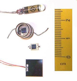
A photodiode is a semiconductor diode sensitive to photon radiation, such as visible light, infrared or ultraviolet radiation, X-rays and gamma rays. It produces an electrical current when it absorbs photons. This can be used for detection and measurement applications, or for the generation of electrical power in solar cells. Photodiodes are used in a wide range of applications throughout the electromagnetic spectrum from visible light photocells to gamma ray spectrometers.

<span class="mw-page-title-main">Fabry–Pérot interferometer</span> Optical device with parallel mirrors

In optics, a Fabry–Pérot interferometer (FPI) or etalon is an optical cavity made from two parallel reflecting surfaces. Optical waves can pass through the optical cavity only when they are in resonance with it. It is named after Charles Fabry and Alfred Perot, who developed the instrument in 1899. Etalon is from the French étalon, meaning "measuring gauge" or "standard".

An avalanche photodiode (APD) is a highly sensitive semiconductor photodiode detector that exploits the photoelectric effect to convert light into electricity. From a functional standpoint, they can be regarded as the semiconductor analog of photomultiplier tubes. The avalanche photodiode was invented by Japanese engineer Jun-ichi Nishizawa in 1952. However, study of avalanche breakdown, microplasma defects in silicon and germanium and the investigation of optical detection using p-n junctions predate this patent. Typical applications for APDs are laser rangefinders, long-range fiber-optic telecommunication, and quantum sensing for control algorithms. New applications include positron emission tomography and particle physics.

Tunable diode laser absorption spectroscopy is a technique for measuring the concentration of certain species such as methane, water vapor and many more, in a gaseous mixture using tunable diode lasers and laser absorption spectrometry. The advantage of TDLAS over other techniques for concentration measurement is its ability to achieve very low detection limits. Apart from concentration, it is also possible to determine the temperature, pressure, velocity and mass flux of the gas under observation. TDLAS is by far the most common laser based absorption technique for quantitative assessments of species in gas phase.

Absorbance is defined as "the logarithm of the ratio of incident to transmitted radiant power through a sample ". Alternatively, for samples which scatter light, absorbance may be defined as "the negative logarithm of one minus absorptance, as measured on a uniform sample". The term is used in many technical areas to quantify the results of an experimental measurement. While the term has its origin in quantifying the absorption of light, it is often entangled with quantification of light which is “lost” to a detector system through other mechanisms. What these uses of the term tend to have in common is that they refer to a logarithm of the ratio of a quantity of light incident on a sample or material to that which is detected after the light has interacted with the sample.

<span class="mw-page-title-main">Mach–Zehnder interferometer</span> Device to determine relative phase shift

The Mach–Zehnder interferometer is a device used to determine the relative phase shift variations between two collimated beams derived by splitting light from a single source. The interferometer has been used, among other things, to measure phase shifts between the two beams caused by a sample or a change in length of one of the paths. The apparatus is named after the physicists Ludwig Mach and Ludwig Zehnder; Zehnder's proposal in an 1891 article was refined by Mach in an 1892 article. Demonstrations of Mach–Zehnder interferometry with particles other than photons had been demonstrated as well in multiple experiments.

<span class="mw-page-title-main">Quantum efficiency</span> Property of photosensitive devices

The term quantum efficiency (QE) may apply to incident photon to converted electron (IPCE) ratio of a photosensitive device, or it may refer to the TMR effect of a magnetic tunnel junction.

<span class="mw-page-title-main">Photodetector</span> Sensors of light or other electromagnetic energy

Photodetectors, also called photosensors, are sensors of light or other electromagnetic radiation. There are a wide variety of photodetectors which may be classified by mechanism of detection, such as photoelectric or photochemical effects, or by various performance metrics, such as spectral response. Semiconductor-based photodetectors typically use a p–n junction that converts photons into charge. The absorbed photons make electron–hole pairs in the depletion region. Photodiodes and photo transistors are a few examples of photo detectors. Solar cells convert some of the light energy absorbed into electrical energy.

<span class="mw-page-title-main">Two-photon absorption</span> Simultaneous absorption of two photons by a molecule

In atomic physics, two-photon absorption, also called two-photon excitation or non-linear absorption, is the simultaneous absorption of two photons of identical or different frequencies in order to excite a molecule from one state to a higher energy, most commonly an excited electronic state. Absorption of two photons with different frequencies is called non-degenerate two-photon absorption. Since TPA depends on the simultaneous absorption of two photons, the probability of TPA is proportional to the square of the light intensity; thus it is a nonlinear optical process. The energy difference between the involved lower and upper states of the molecule is equal or smaller than the sum of the photon energies of the two photons absorbed. Two-photon absorption is a third-order process, with absorption cross section typically several orders of magnitude smaller than one-photon absorption cross section.

<span class="mw-page-title-main">Prism compressor</span>

A prism compressor is an optical device used to shorten the duration of a positively chirped ultrashort laser pulse by giving different wavelength components a different time delay. It typically consists of two prisms and a mirror. Figure 1 shows the construction of such a compressor. Although the dispersion of the prism material causes different wavelength components to travel along different paths, the compressor is built such that all wavelength components leave the compressor at different times, but in the same direction. If the different wavelength components of a laser pulse were already separated in time, the prism compressor can make them overlap with each other, thus causing a shorter pulse.

An LC circuit can be quantized using the same methods as for the quantum harmonic oscillator. An LC circuit is a variety of resonant circuit, and consists of an inductor, represented by the letter L, and a capacitor, represented by the letter C. When connected together, an electric current can alternate between them at the circuit's resonant frequency:

<span class="mw-page-title-main">Quantum well infrared photodetector</span>

A Quantum Well Infrared Photodetector (QWIP) is an infrared photodetector, which uses electronic intersubband transitions in quantum wells to absorb photons. In order to be used for infrared detection, the parameters of the quantum wells in the quantum well infrared photodetector are adjusted so that the energy difference between its first and second quantized states match the incoming infrared photon energy. QWIPs are typically made of gallium arsenide, a material commonly found in smartphones and high-speed communications equipment. Depending on the material and the design of the quantum wells, the energy levels of the QWIP can be tailored to absorb radiation in the infrared region from 3 to 20 µm.

Incoherent broad band cavity enhanced absorption spectroscopy (IBBCEAS), sometimes called broadband cavity enhanced extinction spectroscopy (IBBCEES), measures the transmission of light intensity through a stable optical cavity consisting of high reflectance mirrors (typically R>99.9%). The technique is realized using incoherent sources of radiation e.g. Xenon arc lamps, LEDs or supercontinuum (SC) lasers, hence the name.

Linear optical quantum computing or linear optics quantum computation (LOQC), also photonic quantum computing (PQC), is a paradigm of quantum computation, allowing (under certain conditions, described below) universal quantum computation. LOQC uses photons as information carriers, mainly uses linear optical elements, or optical instruments (including reciprocal mirrors and waveplates) to process quantum information, and uses photon detectors and quantum memories to detect and store quantum information.

References

[1] Goedbloed and Joosten; " Thin Silicon Film p-i-n Photodiodes with Internal Reflection"; IEEE Journal of Solid-State Circuits, 173 – 179, Volume: 13 Issue: 1, Feb (1978).
[2] R G Hunsperger, Integrated Optics: Theory and Technology ispringer, New York, (1991).
[3] M. Selim Unlu, Samuel Strite; "Resonant cavity enhanced photonic devices"; J. Appl. Phys. 78, 607 (1995).
[4] K. Kishino. M. S. Unlu, J. I. Chyi, J. Reed, L. Arsenault, and H. Morkoc; " Resonant Cavity Enhanced Photodetectors", IEEE J. Quantum Electron. 27, 2025 (1991).
[5] A. G. Dentai, R. Kuchibohlta, I. C. Campbell, C. Tsai, C. Lei; "HIGH QUANTUM EFFICIENCY, LONG WAVELENGTH InP/lnGaAs MICROCAVITY PHOTODIODE", 7 November 1991 Vol. 27 No 23.
[6] Ravi Kuchibhotla, Joe C. Campbell, John C. Bean, Larry Peticolas, and Robert Hull; "Si0.8Ge0.2 /Si Bragg-reflector mirrors :for optoelectronic device applications"; Appl. Phys. Lett. 62 (18), 3 May 1993.
[7] F. Y. Huangja, A. Salvador, X. Gui, N. Teraguchi, and H. Morkoq; "Resonant-cavity GaAs/lnGaAs/AIAs photodiodes with a:periodic absorber structure"; Appi. Phys. L&t. 63 (2), 12 July 1993.
[8] R. Kuchibhotla; A. Srinivasan; J.C. Campbell; C. Lei; D.G. Deppe; Y.S. He; B.G. Streetman; "Low-voltage high-gain resonant-cavity avalanche photodiode"; 354 – 356, Volume: 3 Issue: 4, IEEE Photonics Technology Letters, April 1991.
[9] Li, Z.-M. Landheer, D. Veilleux, M. Conn, D.R. Surridge, R. Xu, J.M. McDonald; "Analysis of a resonant-cavity enhanced GaAs/AlGaAs MSM photodetector"; 473 – 476, Volume: 4 Issue: 5, IEEE Photonics Technology Letters, May 1992.
[10]S. Unlu, K. Kishino, J. I. Chyi, L. Arsenault, J. Reed, and H. Morkoc; "Wavelength demultiplexing heterojunction phototransistor"; Electron. Lett. 26, 1857 (1990).