Heterojunction

Last updated

A heterojunction is an interface between two layers or regions of dissimilar semiconductors. These semiconducting materials have unequal band gaps as opposed to a homojunction. It is often advantageous to engineer the electronic energy bands in many solid-state device applications, including semiconductor lasers, solar cells and transistors. The combination of multiple heterojunctions together in a device is called a heterostructure, although the two terms are commonly used interchangeably. The requirement that each material be a semiconductor with unequal band gaps is somewhat loose, especially on small length scales, where electronic properties depend on spatial properties. A more modern definition of heterojunction is the interface between any two solid-state materials, including crystalline and amorphous structures of metallic, insulating, fast ion conductor and semiconducting materials.

Contents

Manufacture and applications

Heterojunction manufacturing generally requires the use of molecular beam epitaxy (MBE) [1] or chemical vapor deposition (CVD) technologies in order to precisely control the deposition thickness and create a cleanly lattice-matched abrupt interface. A recent alternative under research is the mechanical stacking of layered materials into van der Waals heterostructures. [2]

Despite their expense, heterojunctions have found use in a variety of specialized applications where their unique characteristics are critical:

Energy band alignment

The three types of semiconductor heterojunctions organized by band alignment. Heterojunction types.png
The three types of semiconductor heterojunctions organized by band alignment.
Band diagram for stradding gap, n-n semiconductor heterojunction at equilibrium. Straddling gap heterojunction band diagram.svg
Band diagram for stradding gap, n-n semiconductor heterojunction at equilibrium.

The behaviour of a semiconductor junction depends crucially on the alignment of the energy bands at the interface. Semiconductor interfaces can be organized into three types of heterojunctions: straddling gap (type I), staggered gap (type II) or broken gap (type III) as seen in the figure. [8] Away from the junction, the band bending can be computed based on the usual procedure of solving Poisson's equation.

Various models exist to predict the band alignment.

The typical method for measuring band offsets is by calculating them from measuring exciton energies in the luminescence spectra. [12]

Effective mass mismatch

When a heterojunction is formed by two different semiconductors, a quantum well can be fabricated due to difference in band structure. In order to calculate the static energy levels within the achieved quantum well, understanding variation or mismatch of the effective mass across the heterojunction becomes substantial. The quantum well defined in the heterojunction can be treated as a finite well potential with width of . In addition, in 1966, Conley et al. [13] and BenDaniel and Duke [14] reported a boundary condition for the envelope function in a quantum well, known as BenDaniel–Duke boundary condition. According to them, the envelope function in a fabricated quantum well must satisfy a boundary condition which states that and are both continuous in interface regions.

Mathematical details worked out for quantum well example.

Using the Schrödinger equation for a finite well with width of and center at 0, the equation for the achieved quantum well can be written as:

Solution for above equations are well-known, only with different(modified) k and [15]

.

At the z = even-parity solution can be gained from

.

By taking derivative of (5) and multiplying both sides by

.

Dividing (6) by (5), even-parity solution function can be obtained,

.

Similarly, for odd-parity solution,

.

For numerical solution, taking derivatives of (7) and (8) gives

even parity:

odd parity:

where .

The difference in effective mass between materials results in a larger difference in ground state energies.

Nanoscale heterojunctions

Image of a nanoscale heterojunction between iron oxide (Fe3O4 -- sphere) and cadmium sulfide (CdS -- rod) taken with a TEM. This staggered gap (type II) offset junction was synthesized by Hunter McDaniel and Dr. Moonsub Shim at the University of Illinois in Urbana-Champaign in 2007. Fe3O4-CdS Nano Heterojunction.JPG
Image of a nanoscale heterojunction between iron oxide (Fe3O4 — sphere) and cadmium sulfide (CdS — rod) taken with a TEM. This staggered gap (type II) offset junction was synthesized by Hunter McDaniel and Dr. Moonsub Shim at the University of Illinois in Urbana-Champaign in 2007.

In quantum dots the band energies are dependent on crystal size due to the quantum size effects. This enables band offset engineering in nanoscale heterostructures. It is possible [16] to use the same materials but change the type of junction, say from straddling (type I) to staggered (type II), by changing the size or thickness of the crystals involved. The most common nanoscale heterostructure system is ZnS on CdSe (CdSe@ZnS) which has a straddling gap (type I) offset. In this system the much larger band gap ZnS passivates the surface of the fluorescent CdSe core thereby increasing the quantum efficiency of the luminescence. There is an added bonus of increased thermal stability due to the stronger bonds in the ZnS shell as suggested by its larger band gap. Since CdSe and ZnS both grow in the zincblende crystal phase and are closely lattice matched, core shell growth is preferred. In other systems or under different growth conditions it may be possible to grow anisotropic structures such as the one seen in the image on the right.

It has been shown [17] that the driving force for charge transfer between conduction bands in these structures is the conduction band offset. By decreasing the size of CdSe nanocrystals grown on TiO2, Robel et al. [17] found that electrons transferred faster from the higher CdSe conduction band into TiO2. In CdSe the quantum size effect is much more pronounced in the conduction band due to the smaller effective mass than in the valence band, and this is the case with most semiconductors. Consequently, engineering the conduction band offset is typically much easier with nanoscale heterojunctions. For staggered (type II) offset nanoscale heterojunctions, photoinduced charge separation can occur since there the lowest energy state for holes may be on one side of the junction whereas the lowest energy for electrons is on the opposite side. It has been suggested [17] that anisotropic staggered gap (type II) nanoscale heterojunctions may be used for photocatalysis, specifically for water splitting with solar energy.

See also

Related Research Articles

<span class="mw-page-title-main">Particle in a box</span> Mathematical model in quantum mechanics

In quantum mechanics, the particle in a box model describes a particle free to move in a small space surrounded by impenetrable barriers. The model is mainly used as a hypothetical example to illustrate the differences between classical and quantum systems. In classical systems, for example, a particle trapped inside a large box can move at any speed within the box and it is no more likely to be found at one position than another. However, when the well becomes very narrow, quantum effects become important. The particle may only occupy certain positive energy levels. Likewise, it can never have zero energy, meaning that the particle can never "sit still". Additionally, it is more likely to be found at certain positions than at others, depending on its energy level. The particle may never be detected at certain positions, known as spatial nodes.

In solid state physics, a particle's effective mass is the mass that it seems to have when responding to forces, or the mass that it seems to have when interacting with other identical particles in a thermal distribution. One of the results from the band theory of solids is that the movement of particles in a periodic potential, over long distances larger than the lattice spacing, can be very different from their motion in a vacuum. The effective mass is a quantity that is used to simplify band structures by modeling the behavior of a free particle with that mass. For some purposes and some materials, the effective mass can be considered to be a simple constant of a material. In general, however, the value of effective mass depends on the purpose for which it is used, and can vary depending on a number of factors.

<span class="mw-page-title-main">Schottky barrier</span> Potential energy barrier in metal–semiconductor junctions

A Schottky barrier, named after Walter H. Schottky, is a potential energy barrier for electrons formed at a metal–semiconductor junction. Schottky barriers have rectifying characteristics, suitable for use as a diode. One of the primary characteristics of a Schottky barrier is the Schottky barrier height, denoted by ΦB. The value of ΦB depends on the combination of metal and semiconductor.

<span class="mw-page-title-main">Quantum well</span> Concept in quantum mechanics

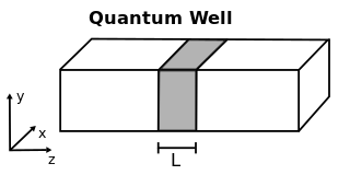
A quantum well is a potential well with only discrete energy values.

In physics, quantum tunnelling, barrier penetration, or simply tunnelling is a quantum mechanical phenomenon in which an object such as an electron or atom passes through a potential energy barrier that, according to classical mechanics, should not be passable due to the object not having sufficient energy to pass or surmount the barrier.

<span class="mw-page-title-main">High-electron-mobility transistor</span> Type of field-effect transistor

A high-electron-mobility transistor, also known as heterostructure FET (HFET) or modulation-doped FET (MODFET), is a field-effect transistor incorporating a junction between two materials with different band gaps as the channel instead of a doped region. A commonly used material combination is GaAs with AlGaAs, though there is wide variation, dependent on the application of the device. Devices incorporating more indium generally show better high-frequency performance, while in recent years, gallium nitride HEMTs have attracted attention due to their high-power performance. Like other FETs, HEMTs are used in integrated circuits as digital on-off switches. FETs can also be used as amplifiers for large amounts of current using a small voltage as a control signal. Both of these uses are made possible by the FET’s unique current–voltage characteristics. HEMT transistors are able to operate at higher frequencies than ordinary transistors, up to millimeter wave frequencies, and are used in high-frequency products such as cell phones, satellite television receivers, voltage converters, and radar equipment. They are widely used in satellite receivers, in low power amplifiers and in the defense industry.

A superlattice is a periodic structure of layers of two materials. Typically, the thickness of one layer is several nanometers. It can also refer to a lower-dimensional structure such as an array of quantum dots or quantum wells.

In solid-state physics of semiconductors, carrier generation and carrier recombination are processes by which mobile charge carriers are created and eliminated. Carrier generation and recombination processes are fundamental to the operation of many optoelectronic semiconductor devices, such as photodiodes, light-emitting diodes and laser diodes. They are also critical to a full analysis of p-n junction devices such as bipolar junction transistors and p-n junction diodes.

Surface states are electronic states found at the surface of materials. They are formed due to the sharp transition from solid material that ends with a surface and are found only at the atom layers closest to the surface. The termination of a material with a surface leads to a change of the electronic band structure from the bulk material to the vacuum. In the weakened potential at the surface, new electronic states can be formed, so called surface states.

A two-dimensional electron gas (2DEG) is a scientific model in solid-state physics. It is an electron gas that is free to move in two dimensions, but tightly confined in the third. This tight confinement leads to quantized energy levels for motion in the third direction, which can then be ignored for most problems. Thus the electrons appear to be a 2D sheet embedded in a 3D world. The analogous construct of holes is called a two-dimensional hole gas (2DHG), and such systems have many useful and interesting properties.

The Franz–Keldysh effect is a change in optical absorption by a semiconductor when an electric field is applied. The effect is named after the German physicist Walter Franz and Russian physicist Leonid Keldysh.

<span class="mw-page-title-main">Anderson's rule</span>

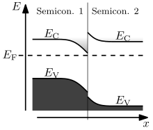
Anderson's rule is used for the construction of energy band diagrams of the heterojunction between two semiconductor materials. Anderson's rule states that when constructing an energy band diagram, the vacuum levels of the two semiconductors on either side of the heterojunction should be aligned.

Band offset describes the relative alignment of the energy bands at a semiconductor heterojunction.

In bulk semiconductor band structure calculations, it is assumed that the crystal lattice of the material is infinite. When the finite size of a crystal is taken into account, the wavefunctions of electrons are altered and states that are forbidden within the bulk semiconductor gap are allowed at the surface. Similarly, when a metal is deposited onto a semiconductor, the wavefunction of an electron in the semiconductor must match that of an electron in the metal at the interface. Since the Fermi levels of the two materials must match at the interface, there exists gap states that decay deeper into the semiconductor.

<span class="mw-page-title-main">Multi-junction solar cell</span> Solar power cell with multiple band gaps from different materials

Multi-junction (MJ) solar cells are solar cells with multiple p–n junctions made of different semiconductor materials. Each material's p-n junction will produce electric current in response to different wavelengths of light. The use of multiple semiconducting materials allows the absorbance of a broader range of wavelengths, improving the cell's sunlight to electrical energy conversion efficiency.

In solid-state physics, the k·p perturbation theory is an approximated semi-empirical approach for calculating the band structure and optical properties of crystalline solids. It is pronounced "k dot p", and is also called the "k·p method". This theory has been applied specifically in the framework of the Luttinger–Kohn model, and of the Kane model.

<span class="mw-page-title-main">Shockley–Queisser limit</span> Maximum theoretical efficiency of a solar cell

In physics, the radiative efficiency limit is the maximum theoretical efficiency of a solar cell using a single p-n junction to collect power from the cell where the only loss mechanism is radiative recombination in the solar cell. It was first calculated by William Shockley and Hans-Joachim Queisser at Shockley Semiconductor in 1961, giving a maximum efficiency of 30% at 1.1 eV. The limit is one of the most fundamental to solar energy production with photovoltaic cells, and is one of the field's most important contributions.

The quantum-confined Stark effect (QCSE) describes the effect of an external electric field upon the light absorption spectrum or emission spectrum of a quantum well (QW). In the absence of an external electric field, electrons and holes within the quantum well may only occupy states within a discrete set of energy subbands. Only a discrete set of frequencies of light may be absorbed or emitted by the system. When an external electric field is applied, the electron states shift to lower energies, while the hole states shift to higher energies. This reduces the permitted light absorption or emission frequencies. Additionally, the external electric field shifts electrons and holes to opposite sides of the well, decreasing the overlap integral, which in turn reduces the recombination efficiency of the system. The spatial separation between the electrons and holes is limited by the presence of the potential barriers around the quantum well, meaning that excitons are able to exist in the system even under the influence of an electric field. The quantum-confined Stark effect is used in QCSE optical modulators, which allow optical communications signals to be switched on and off rapidly.

The Monte Carlo method for electron transport is a semiclassical Monte Carlo (MC) approach of modeling semiconductor transport. Assuming the carrier motion consists of free flights interrupted by scattering mechanisms, a computer is utilized to simulate the trajectories of particles as they move across the device under the influence of an electric field using classical mechanics. The scattering events and the duration of particle flight is determined through the use of random numbers.

<span class="mw-page-title-main">Phonovoltaic</span>

A phonovoltaic (pV) cell converts vibrational (phonons) energy into a direct current much like the photovoltaic effect in a photovoltaic (PV) cell converts light (photon) into power. That is, it uses a p-n junction to separate the electrons and holes generated as valence electrons absorb optical phonons more energetic than the band gap, and then collects them in the metallic contacts for use in a circuit. The pV cell is an application of heat transfer physics and competes with other thermal energy harvesting devices like the thermoelectric generator.

References

  1. 1 2 Smith, C.G (1996). "Low-dimensional quantum devices". Rep. Prog. Phys. 59 (1996) 235282, pg 244.
  2. Geim, A. K.; Grigorieva, I. V. (2013). "Van der Waals heterostructures". Nature. 499 (7459): 419–425. arXiv: 1307.6718 . doi:10.1038/nature12385. ISSN   0028-0836. PMID   23887427. S2CID   205234832.
  3. Leu, Sylvère; Sontag, Detlef (2020), Shah, Arvind (ed.), "Crystalline Silicon Solar Cells: Heterojunction Cells", Solar Cells and Modules, vol. 301, Cham: Springer International Publishing, pp. 163–195, doi:10.1007/978-3-030-46487-5_7, ISBN   978-3-030-46485-1 , retrieved 2023-04-18
  4. Okuda, Koji; Okamoto, Hiroaki; Hamakawa, Yoshihiro (1983). "Amorphous Si/Polycrystalline Si Stacked Solar Cell Having More Than 12% Conversion Efficiency". Japanese Journal of Applied Physics. 22 (9): L605–L607. Bibcode:1983JaJAP..22L.605O. doi:10.1143/JJAP.22.L605. S2CID   121569675.
  5. Yamamoto, Kenji; Yoshikawa, Kunta; Uzu, Hisashi; Adachi, Daisuke (2018). "High-efficiency heterojunction crystalline Si solar cells". Japanese Journal of Applied Physics. 57 (8S3): 08RB20. Bibcode:2018JaJAP..57hRB20Y. doi:10.7567/JJAP.57.08RB20. S2CID   125265042.
  6. "HJT - Heterojunction Solar Cells". Solar Power Panels. Retrieved 2022-03-25.
  7. Kroemer, H. (1963). "A proposed class of hetero-junction injection lasers". Proceedings of the IEEE. 51 (12): 1782–1783. doi:10.1109/PROC.1963.2706.
  8. Ihn, Thomas (2010). "ch. 5.1 Band engineering". Semiconductor Nanostructures Quantum States and Electronic Transport . United States of America: Oxford University Press. pp.  66. ISBN   9780199534432.
  9. J. Tersoff (1984). "Theory of semiconductor heterojunctions: The role of quantum dipoles". Physical Review B. 30 (8): 4874–4877. Bibcode:1984PhRvB..30.4874T. doi:10.1103/PhysRevB.30.4874.
  10. Pallab, Bhattacharya (1997), Semiconductor Optoelectronic Devices, Prentice Hall, ISBN   0-13-495656-7
  11. Adachi, Sadao (1993-01-01). Properties of Aluminium Gallium Arsenide. ISBN   9780852965580.
  12. 1 2 Debbar, N.; Biswas, Dipankar; Bhattacharya, Pallab (1989). "Conduction-band offsets in pseudomorphic InxGa1-xAs/Al0.2Ga0.8As quantum wells (0.07≤x≤0.18) measured by deep-level transient spectroscopy". Physical Review B. 40 (2): 1058–1063. Bibcode:1989PhRvB..40.1058D. doi:10.1103/PhysRevB.40.1058. PMID   9991928.
  13. Conley, J.; Duke, C.; Mahan, G.; Tiemann, J. (1966). "Electron Tunneling in Metal–Semiconductor Barriers". Physical Review. 150 (2): 466. Bibcode:1966PhRv..150..466C. doi:10.1103/PhysRev.150.466.
  14. Bendaniel, D.; Duke, C. (1966). "Space-Charge Effects on Electron Tunneling". Physical Review. 152 (2): 683. Bibcode:1966PhRv..152..683B. doi:10.1103/PhysRev.152.683.
  15. Griffiths, David J. (2004). Introduction to Quantum Mechanics (2nd ed.). Prentice Hall. ISBN   0-13-111892-7
  16. Ivanov, Sergei A.; Piryatinski, Andrei; Nanda, Jagjit; Tretiak, Sergei; Zavadil, Kevin R.; Wallace, William O.; Werder, Don; Klimov, Victor I. (2007). "Type-II Core/Shell CdS/ZnSe Nanocrystals: Synthesis, Electronic Structures, and Spectroscopic Properties". Journal of the American Chemical Society. 129 (38): 11708–19. doi:10.1021/ja068351m. PMID   17727285.
  17. 1 2 3 Robel, István; Kuno, Masaru; Kamat, Prashant V. (2007). "Size-Dependent Electron Injection from Excited CdSe Quantum Dots into TiO2Nanoparticles". Journal of the American Chemical Society. 129 (14): 4136–7. doi:10.1021/ja070099a. PMID   17373799.

Further reading