Electron hole

Last updated
When an electron leaves a helium atom, it leaves an electron hole in its place. This causes the helium atom to become positively charged. Electron-hole.svg
When an electron leaves a helium atom, it leaves an electron hole in its place. This causes the helium atom to become positively charged.

In physics, chemistry, and electronic engineering, an electron hole (often simply called a hole) is a quasiparticle denoting the lack of an electron at a position where one could exist in an atom or atomic lattice. Since in a normal atom or crystal lattice the negative charge of the electrons is balanced by the positive charge of the atomic nuclei, the absence of an electron leaves a net positive charge at the hole's location.

Contents

Holes in a metal [1] or semiconductor crystal lattice can move through the lattice as electrons can, and act similarly to positively-charged particles. They play an important role in the operation of semiconductor devices such as transistors, diodes (including light-emitting diodes) and integrated circuits. If an electron is excited into a higher state it leaves a hole in its old state. This meaning is used in Auger electron spectroscopy (and other x-ray techniques), in computational chemistry, and to explain the low electron-electron scattering-rate in crystals (metals and semiconductors). Although they act like elementary particles, holes are rather quasiparticles; they are different from the positron, which is the antiparticle of the electron. (See also Dirac sea.)

In crystals, electronic band structure calculations lead to an effective mass for the electrons that is typically negative at the top of a band. The negative mass is an unintuitive concept, [2] and in these situations, a more familiar picture is found by considering a positive charge with a positive mass.

Solid-state physics

In solid-state physics, an electron hole (usually referred to simply as a hole) is the absence of an electron from a full valence band. A hole is essentially a way to conceptualize the interactions of the electrons within a nearly full valence band of a crystal lattice, which is missing a small fraction of its electrons. In some ways, the behavior of a hole within a semiconductor crystal lattice is comparable to that of the bubble in a full bottle of water. [3]

The hole concept was pioneered in 1929 by Rudolf Peierls, who analyzed the Hall effect using Bloch's theorem, and demonstrated that a nearly full and a nearly empty Brillouin zones give the opposite Hall voltages. The concept of an electron hole in solid-state physics predates the concept of a hole in Dirac equation, but there is no evidence that it would have influenced Dirac's thinking. [4]

Simplified analogy: Empty seat in an auditorium

A children's puzzle which illustrates the mobility of holes in an atomic lattice. The tiles are analogous to electrons, while the missing tile (lower right corner) is analogous to a hole. Just as the position of the missing tile can be moved to different locations by moving the tiles, a hole in a crystal lattice can move to different positions in the lattice by the motion of the surrounding electrons. 15-puzzle-02.jpg
A children's puzzle which illustrates the mobility of holes in an atomic lattice. The tiles are analogous to electrons, while the missing tile (lower right corner) is analogous to a hole. Just as the position of the missing tile can be moved to different locations by moving the tiles, a hole in a crystal lattice can move to different positions in the lattice by the motion of the surrounding electrons.

Hole conduction in a valence band can be explained by the following analogy:

Imagine a row of people seated in an auditorium, where there are no spare chairs. Someone in the middle of the row wants to leave, so he jumps over the back of the seat into another row, and walks out. The empty row is analogous to the conduction band, and the person walking out is analogous to a conduction electron.

Now imagine someone else comes along and wants to sit down. The empty row has a poor view; so he does not want to sit there. Instead, a person in the crowded row moves into the empty seat the first person left behind. The empty seat moves one spot closer to the edge and the person waiting to sit down. The next person follows, and the next, et cetera. One could say that the empty seat moves towards the edge of the row. Once the empty seat reaches the edge, the new person can sit down.

In the process everyone in the row has moved along. If those people were negatively charged (like electrons), this movement would constitute conduction. If the seats themselves were positively charged, then only the vacant seat would be positive. This is a very simple model of how hole conduction works.

Instead of analyzing the movement of an empty state in the valence band as the movement of many separate electrons, a single equivalent imaginary particle called a "hole" is considered. In an applied electric field, the electrons move in one direction, corresponding to the hole moving in the other. If a hole associates itself with a neutral atom, that atom loses an electron and becomes positive. Therefore, the hole is taken to have positive charge of +e, precisely the opposite of the electron charge.

In reality, due to the uncertainty principle of quantum mechanics, combined with the energy levels available in the crystal, the hole is not localizable to a single position as described in the previous example. Rather, the positive charge which represents the hole spans an area in the crystal lattice covering many hundreds of unit cells. This is equivalent to being unable to tell which broken bond corresponds to the "missing" electron. Conduction band electrons are similarly delocalized.

Detailed picture: A hole is the absence of a negative-mass electron

A semiconductor electronic band structure (right) includes the dispersion relation of each band, i.e. the energy of an electron E as a function of the electron's wavevector k. The "unfilled band" is the semiconductor's conduction band; it curves upward indicating positive effective mass. The "filled band" is the semiconductor's valence band; it curves downward indicating negative effective mass. BandDiagram-Semiconductors-E.PNG
A semiconductor electronic band structure (right) includes the dispersion relation of each band, i.e. the energy of an electron E as a function of the electron's wavevector k. The "unfilled band" is the semiconductor's conduction band; it curves upward indicating positive effective mass. The "filled band" is the semiconductor's valence band; it curves downward indicating negative effective mass.

The analogy above is quite simplified, and cannot explain why holes create an opposite effect to electrons in the Hall effect and Seebeck effect. A more precise and detailed explanation follows. [5]

The dispersion relation determines how electrons respond to forces (via the concept of effective mass). [5]

A dispersion relation is the relationship between wavevector (k-vector) and energy in a band, part of the electronic band structure. In quantum mechanics, the electrons are waves, and energy is the wave frequency. A localized electron is a wavepacket, and the motion of an electron is given by the formula for the group velocity of a wave. An electric field affects an electron by gradually shifting all the wavevectors in the wavepacket, and the electron accelerates when its wave group velocity changes. Therefore, again, the way an electron responds to forces is entirely determined by its dispersion relation. An electron floating in space has the dispersion relation E = ℏ2k2/(2m), where m is the (real) electron mass and ℏ is reduced Planck constant. Near the bottom of the conduction band of a semiconductor, the dispersion relation is instead E = ℏ2k2/(2m*) (m* is the effective mass ), so a conduction-band electron responds to forces as if it had the mass m*.

Electrons near the top of the valence band behave as if they have negative mass. [5]

The dispersion relation near the top of the valence band is E = ℏ2k2/(2m*) with negative effective mass. So electrons near the top of the valence band behave like they have negative mass. When a force pulls the electrons to the right, these electrons actually move left. This is solely due to the shape of the valence band and is unrelated to whether the band is full or empty. If you could somehow empty out the valence band and just put one electron near the valence band maximum (an unstable situation), this electron would move the "wrong way" in response to forces.

Positively-charged holes as a shortcut for calculating the total current of an almost-full band. [5]

A perfectly full band always has zero current. One way to think about this fact is that the electron states near the top of the band have negative effective mass, and those near the bottom of the band have positive effective mass, so the net motion is exactly zero. If an otherwise-almost-full valence band has a state without an electron in it, we say that this state is occupied by a hole. There is a mathematical shortcut for calculating the current due to every electron in the whole valence band: Start with zero current (the total if the band were full), and subtract the current due to the electrons that would be in each hole state if it wasn't a hole. Since subtracting the current caused by a negative charge in motion is the same as adding the current caused by a positive charge moving on the same path, the mathematical shortcut is to pretend that each hole state is carrying a positive charge, while ignoring every other electron state in the valence band.

A hole near the top of the valence band moves the same way as an electron near the top of the valence band would move [5] (which is in the opposite direction compared to conduction-band electrons experiencing the same force.)

This fact follows from the discussion and definition above. This is an example where the auditorium analogy above is misleading. When a person moves left in a full auditorium, an empty seat moves right. But in this section we are imagining how electrons move through k-space, not real space, and the effect of a force is to move all the electrons through k-space in the same direction at the same time. In this context, a better analogy is a bubble underwater in a river: The bubble moves the same direction as the water, not the opposite.

Since force = mass × acceleration, a negative-effective-mass electron near the top of the valence band would move the opposite direction as a positive-effective-mass electron near the bottom of the conduction band, in response to a given electric or magnetic force. Therefore, a hole moves this way as well.

Conclusion: Hole is a positive-charge, positive-mass quasiparticle .

From the above, a hole (1) carries a positive charge, and (2) responds to electric and magnetic fields as if it had a positive charge and positive mass. (The latter is because a particle with positive charge and positive mass respond to electric and magnetic fields in the same way as a particle with a negative charge and negative mass.) That explains why holes can be treated in all situations as ordinary positively charged quasiparticles.

Role in semiconductor technology

An array of Silicon atoms doped with Boron creates holes. This type of extrinsic semiconducting material is dubbed Type P. Silicon doping - Type P.svg
An array of Silicon atoms doped with Boron creates holes. This type of extrinsic semiconducting material is dubbed Type P.

In some semiconductors, such as silicon, the hole's effective mass is dependent on a direction (anisotropic), however a value averaged over all directions can be used for some macroscopic calculations.

In most semiconductors, the effective mass of a hole is much larger than that of an electron. This results in lower mobility for holes under the influence of an electric field and this may slow down the speed of the electronic device made of that semiconductor. This is one major reason for adopting electrons as the primary charge carriers, whenever possible in semiconductor devices, rather than holes. This is also why NMOS logic is faster than PMOS logic. OLED screens have been modified to reduce imbalance resulting in non radiative recombination by adding extra layers and/or decreasing electron density on one plastic layer so electrons and holes precisely balance within the emission zone. However, in many semiconductor devices, both electrons and holes play an essential role. Examples include p–n diodes, bipolar transistors, and CMOS logic.

Holes in quantum chemistry

An alternate meaning for the term electron hole is used in computational chemistry. In coupled cluster methods, the ground (or lowest energy) state of a molecule is interpreted as the "vacuum state"—conceptually, in this state, there are no electrons. In this scheme, the absence of an electron from a normally filled state is called a "hole" and is treated as a particle, and the presence of an electron in a normally empty state is simply called an "electron". This terminology is almost identical to that used in solid-state physics.

See also

Related Research Articles

<span class="mw-page-title-main">Electric current</span> Flow of electric charge

An electric current is a flow of charged particles, such as electrons or ions, moving through an electrical conductor or space. It is defined as the net rate of flow of electric charge through a surface. The moving particles are called charge carriers, which may be one of several types of particles, depending on the conductor. In electric circuits the charge carriers are often electrons moving through a wire. In semiconductors they can be electrons or holes. In an electrolyte the charge carriers are ions, while in plasma, an ionized gas, they are ions and electrons.

A semiconductor is a material that has an electrical conductivity value falling between that of a conductor, such as copper, and an insulator, such as glass. Its resistivity generally falls as its temperature rises; metals behave in the opposite way. In many cases their conducting properties may be altered in useful ways by introducing impurities ("doping") into the crystal structure. When two differently doped regions exist in the same crystal, a semiconductor junction is created. The behavior of charge carriers, which include electrons, ions, and electron holes, at these junctions is the basis of diodes, transistors, and most modern electronics. Some examples of semiconductors are silicon, germanium, gallium arsenide, and elements near the so-called "metalloid staircase" on the periodic table. After silicon, gallium arsenide is the second-most common semiconductor and is used in laser diodes, solar cells, microwave-frequency integrated circuits, and others. Silicon is a critical element for fabricating most electronic circuits.

<span class="mw-page-title-main">Exciton</span> Quasiparticle which is a bound state of an electron and an electron hole

An electron and an electron hole that are attracted to each other by the Coulomb force can form a bound state called an exciton. It is an electrically neutral quasiparticle that exists mainly in condensed matter, including insulators, semiconductors, some metals, but also in certain atoms, molecules and liquids. The exciton is regarded as an elementary excitation that can transport energy without transporting net electric charge.

<span class="mw-page-title-main">Band gap</span> Energy range in a solid where no electron states exist

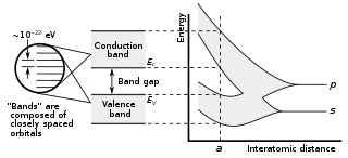
In solid-state physics and solid-state chemistry, a band gap, also called a bandgap or energy gap, is an energy range in a solid where no electronic states exist. In graphs of the electronic band structure of solids, the band gap refers to the energy difference between the top of the valence band and the bottom of the conduction band in insulators and semiconductors. It is the energy required to promote an electron from the valence band to the conduction band. The resulting conduction-band electron are free to move within the crystal lattice and serve as charge carriers to conduct electric current. It is closely related to the HOMO/LUMO gap in chemistry. If the valence band is completely full and the conduction band is completely empty, then electrons cannot move within the solid because there are no available states. If the electrons are not free to move within the crystal lattice, then there is no generated current due to no net charge carrier mobility. However, if some electrons transfer from the valence band to the conduction band, then current can flow. Therefore, the band gap is a major factor determining the electrical conductivity of a solid. Substances having large band gaps are generally insulators, those with small band gaps are semiconductor, and conductors either have very small band gaps or none, because the valence and conduction bands overlap to form a continuous band.

In solid state physics, a particle's effective mass is the mass that it seems to have when responding to forces, or the mass that it seems to have when interacting with other identical particles in a thermal distribution. One of the results from the band theory of solids is that the movement of particles in a periodic potential, over long distances larger than the lattice spacing, can be very different from their motion in a vacuum. The effective mass is a quantity that is used to simplify band structures by modeling the behavior of a free particle with that mass. For some purposes and some materials, the effective mass can be considered to be a simple constant of a material. In general, however, the value of effective mass depends on the purpose for which it is used, and can vary depending on a number of factors.

The electron affinity (Eea) of an atom or molecule is defined as the amount of energy released when an electron attaches to a neutral atom or molecule in the gaseous state to form an anion.

<span class="mw-page-title-main">Dirac sea</span> Theoretical model of the vacuum

The Dirac sea is a theoretical model of the electron vacuum as an infinite sea of electrons with negative energy, now called positrons. It was first postulated by the British physicist Paul Dirac in 1930 to explain the anomalous negative-energy quantum states predicted by the Dirac equation for relativistic electrons. The positron, the antimatter counterpart of the electron, was originally conceived of as a hole in the Dirac sea, before its experimental discovery in 1932.

In physics, a charge carrier is a particle or quasiparticle that is free to move, carrying an electric charge, especially the particles that carry electric charges in electrical conductors. Examples are electrons, ions and holes. The term is used most commonly in solid state physics. In a conducting medium, an electric field can exert force on these free particles, causing a net motion of the particles through the medium; this is what constitutes an electric current. The electron and the proton are the elementary charge carriers, each carrying one elementary charge (e), of the same magnitude and opposite sign.

<span class="mw-page-title-main">Quantum well</span> Concept in quantum mechanics

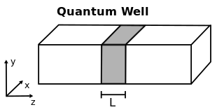
A quantum well is a potential well with only discrete energy values.

In condensed matter physics, a quasiparticle is a concept used to describe a collective behavior of a group of particles that can be treated as if they were a single particle. Formally, quasiparticles and collective excitations are closely related phenomena that arise when a microscopically complicated system such as a solid behaves as if it contained different weakly interacting particles in vacuum.

In solid-state physics, the electronic band structure of a solid describes the range of energy levels that electrons may have within it, as well as the ranges of energy that they may not have.

<span class="mw-page-title-main">Semimetal</span>

A semimetal is a material with a very small overlap between the bottom of the conduction band and the top of the valence band. According to electronic band theory, solids can be classified as insulators, semiconductors, semimetals, or metals. In insulators and semiconductors the filled valence band is separated from an empty conduction band by a band gap. For insulators, the magnitude of the band gap is larger than that of a semiconductor. Because of the slight overlap between the conduction and valence bands, semimetals have no band gap and a negligible density of states at the Fermi level. A metal, by contrast, has an appreciable density of states at the Fermi level because the conduction band is partially filled.

In solid-state physics, the free electron model is a quantum mechanical model for the behaviour of charge carriers in a metallic solid. It was developed in 1927, principally by Arnold Sommerfeld, who combined the classical Drude model with quantum mechanical Fermi–Dirac statistics and hence it is also known as the Drude–Sommerfeld model.

A superlattice is a periodic structure of layers of two materials. Typically, the thickness of one layer is several nanometers. It can also refer to a lower-dimensional structure such as an array of quantum dots or quantum wells.

In the solid-state physics of semiconductors, carrier generation and carrier recombination are processes by which mobile charge carriers are created and eliminated. Carrier generation and recombination processes are fundamental to the operation of many optoelectronic semiconductor devices, such as photodiodes, light-emitting diodes and laser diodes. They are also critical to a full analysis of p-n junction devices such as bipolar junction transistors and p-n junction diodes.

An intrinsic semiconductor, also called a pure semiconductor, undoped semiconductor or i-type semiconductor, is a semiconductor without any significant dopant species present. The number of charge carriers is therefore determined by the properties of the material itself instead of the amount of impurities. In intrinsic semiconductors the number of excited electrons and the number of holes are equal: n = p. This may be the case even after doping the semiconductor, though only if it is doped with both donors and acceptors equally. In this case, n = p still holds, and the semiconductor remains intrinsic, though doped. This means that some conductors are both intrinsic as well as extrinsic but only if n is equal to p.

An extrinsic semiconductor is one that has been doped; during manufacture of the semiconductor crystal a trace element or chemical called a doping agent has been incorporated chemically into the crystal, for the purpose of giving it different electrical properties than the pure semiconductor crystal, which is called an intrinsic semiconductor. In an extrinsic semiconductor it is these foreign dopant atoms in the crystal lattice that mainly provide the charge carriers which carry electric current through the crystal. The doping agents used are of two types, resulting in two types of extrinsic semiconductor. An electron donor dopant is an atom which, when incorporated in the crystal, releases a mobile conduction electron into the crystal lattice. An extrinsic semiconductor that has been doped with electron donor atoms is called an n-type semiconductor, because the majority of charge carriers in the crystal are negative electrons. An electron acceptor dopant is an atom which accepts an electron from the lattice, creating a vacancy where an electron should be called a hole which can move through the crystal like a positively charged particle. An extrinsic semiconductor which has been doped with electron acceptor atoms is called a p-type semiconductor, because the majority of charge carriers in the crystal are positive holes.

<span class="mw-page-title-main">Direct and indirect band gaps</span> Types of energy range in a solid where no electron states can exist

In semiconductor physics, the band gap of a semiconductor can be of two basic types, a direct band gap or an indirect band gap. The minimal-energy state in the conduction band and the maximal-energy state in the valence band are each characterized by a certain crystal momentum (k-vector) in the Brillouin zone. If the k-vectors are different, the material has an "indirect gap". The band gap is called "direct" if the crystal momentum of electrons and holes is the same in both the conduction band and the valence band; an electron can directly emit a photon. In an "indirect" gap, a photon cannot be emitted because the electron must pass through an intermediate state and transfer momentum to the crystal lattice.

<span class="mw-page-title-main">Field effect (semiconductor)</span>

In physics, the field effect refers to the modulation of the electrical conductivity of a material by the application of an external electric field.

<span class="mw-page-title-main">Valence and conduction bands</span> Electron energy bands which determine the electrical conductivity of a material

In solid-state physics, the valence band and conduction band are the bands closest to the Fermi level, and thus determines the electrical conductivity of the solid. In nonmetals, the valence band is the highest range of electron energies in which electrons are normally present at absolute zero temperature, while the conduction band is the lowest range of vacant electronic states. On a graph of the electronic band structure of a semiconducting material, the valence band is located below the Fermi level, while the conduction band is located above it.

References

  1. Ashcroft and Mermin (1976). Solid State Physics (1st ed.). Holt, Rinehart, and Winston. pp.  299–302. ISBN   978-0-03-083993-1.
  2. For these negative mass electrons, momentum is opposite to velocity, so forces acting on these electrons cause their velocity to change in the 'wrong' direction. As these electrons gain energy (moving towards the top of the band), they slow down.
  3. Weller, Paul F. (1967). "An analogy for elementary band theory concepts in solids". J. Chem. Educ. 44 (7): 391. Bibcode:1967JChEd..44..391W. doi:10.1021/ed044p391.
  4. Pippard, Brian (1995). "Electrons in solids". Twentieth century physics. Vol. III. American Institute of Physics Press. pp. 1296–1298. ISBN   978-0-7503-0310-1.
  5. 1 2 3 4 5 Kittel, Introduction to Solid State Physics , 8th edition, pp. 194–196.