Band bending

Last updated

In solid-state physics, band bending refers to the process in which the electronic band structure in a material curves up or down near a junction or interface. It does not involve any physical (spatial) bending. When the electrochemical potential of the free charge carriers around an interface of a semiconductor is dissimilar, charge carriers are transferred between the two materials until an equilibrium state is reached whereby the potential difference vanishes. [1] The band bending concept was first developed in 1938 when Mott, Davidov and Schottky all published theories of the rectifying effect of metal-semiconductor contacts. [2] [3] The use of semiconductor junctions sparked the computer revolution in 1990. Devices such as the diode, the transistor, the photocell and many more still play an important role in technology.

Contents

Qualitative description

Band bending can be induced by several types of contact. In this section metal-semiconductor contact, surface state, applied bias and adsorption induced band bending are discussed.

Figure 1: Energy band diagrams of the surface contact between metals and n-type semiconductors.
E
v
a
c
{\displaystyle E_{vac}}
, the vacuum energy;
E
v
{\displaystyle E_{v}}
, the maximum energy of the valence band;
E
c
{\displaystyle E_{c}}
, minimum energy of the conduction band;
ph
m
{\displaystyle \phi _{m}}
, the metal work function;
ph
s
{\displaystyle \phi _{s}}
, the semiconductor work function;
kh
s
{\displaystyle \chi _{s}}
, the electron affinity of the semiconductor. Band bending.png
Figure 1: Energy band diagrams of the surface contact between metals and n-type semiconductors. , the vacuum energy; , the maximum energy of the valence band; , minimum energy of the conduction band; , the metal work function; , the semiconductor work function; , the electron affinity of the semiconductor.

Metal-semiconductor contact induced band bending

Figure 1 shows the ideal band diagram (i.e. the band diagram at zero temperature without any impurities, defects or contaminants) of a metal with an n-type semiconductor before (top) and after contact (bottom). The work function is defined as the energy difference between the Fermi level of the material and the vacuum level before contact and is denoted by . When the metal and semiconductor are brought in contact, charge carriers (i.e. free electrons and holes) will transfer between the two materials as a result of the work function difference .

If the metal work function () is larger than that of the semiconductor (), that is , the electrons will flow from the semiconductor to the metal, thereby lowering the semiconductor Fermi level and increasing that of the metal. Under equilibrium the work function difference vanishes and the Fermi levels align across the interface. A Helmholtz double layer will be formed near the junction, in which the metal is negatively charged and the semiconductor is positively charged due to this electrostatic induction. Consequently, a net electric field is established from the semiconductor to the metal. Due to the low concentration of free charge carriers in the semiconductor, the electric field cannot be effectively screened (unlike in the metal where in the bulk). This causes the formation of a depletion region near the semiconductor surface. In this region, the energy band edges in the semiconductor bend upwards as a result of the accumulated charge and the associated electric field between the semiconductor and the metal surface.

In the case of , electrons are shared from the metal to the semiconductor, resulting in an electric field that points in the opposite direction. Hence, the band bending is downward as can be seen in the bottom right of Figure 1.

One can envision the direction of bending by considering the electrostatic energy experienced by an electron as it moves across the interface. When , the metal develops a negative charge. An electron moving from the semiconductor to the metal therefore experiences a growing repulsion as it approaches the interface. It follows that its potential energy rises and hence the band bending is upwards. In the case of , the semiconductor carries a negative charge, forming a so-called accumulation layer and leaving a positive charge on the metal surface. An electric field develops from the metal to the semiconductor which drives the electrons towards the metal. By moving closer to the metal the electron could thus lower its potential energy. The result is that the semiconductor energy band bends downwards towards the metal surface. [4]

Surface state induced band bending
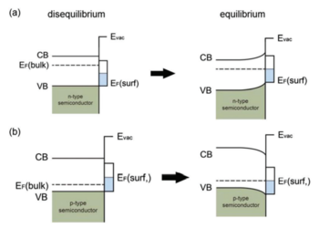
Figure 2: Energy band diagrams under influence of surface-induced band bending. CB, the conduction band; VB, the valence band;
E
F
{\displaystyle E_{F}}
, the Fermi energy;
E
v
a
c
{\displaystyle E_{vac}}
, the vacuum energy. Band bending 2.png
Figure 2: Energy band diagrams under influence of surface-induced band bending. CB, the conduction band; VB, the valence band; , the Fermi energy; , the vacuum energy.

Despite being energetically unfavourable, surface states may exist on a clean semiconductor surface due to the termination of the materials lattice periodicity. Band bending can also be induced in the energy bands of such surface states. A schematic of an ideal band diagram near the surface of a clean semiconductor in and out of equilibrium with its surface states is shown in Figure 2 . The unpaired electrons in the dangling bonds of the surface atoms interact with each other to form an electronic state with a narrow energy band, located somewhere within the band gap of the bulk material. For simplicity, the surface state band is assumed to be half-filled with its Fermi level located at the mid-gap energy of the bulk. Furthermore, doping is taken to not be of influence to the surface states. This is a valid approximation since the dopant concentration is low.

For intrinsic semiconductors (undoped), the valence band is fully filled with electrons, whilst the conduction band is completely empty. The Fermi level is thus located in the middle of the band gap, the same as that of the surface states, and hence there is no charge transfer between the bulk and the surface. As a result no band bending occurs. If the semiconductor is doped, the Fermi level of the bulk is shifted with respect to that of the undoped semiconductor by the introduction of dopant eigenstates within the band gap. It is shifted up for n-doped semiconductors (closer to the conduction band) and down in case of p-doping (nearing the valence band). In disequilibrium, the Fermi energy is thus lower or higher than that of the surface states for p- and n-doping, respectively. Due to the energy difference, electrons will flow from the bulk to the surface or vice versa until the Fermi levels become aligned at equilibrium. The result is that, for n-doping, the energy bands bend upward, whereas they bend downwards for p-doped semiconductors. [5] Note that the density of surface states is large () in comparison with the dopant concentration in the bulk (). Therefore, the Fermi energy of the semiconductor is almost independent of the bulk dopant concentration and is instead determined by the surface states. This is called Fermi level pinning.

Adsorption induced band bending
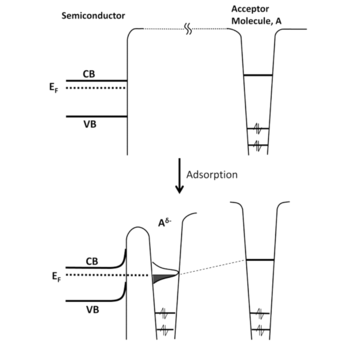
Figure 3: Influence of the adsorption of an acceptor molecule (A) on the surface of an n-type semiconductor . Adsorption band bending.png
Figure 3: Influence of the adsorption of an acceptor molecule (A) on the surface of an n-type semiconductor .

Adsorption on a semiconductor surface can also induce band bending. Figure 3 illustrates the adsorption of an acceptor molecule (A) onto a semiconductor surface. As the molecule approaches the surface, an unfilled molecular orbital of the acceptor interacts with the semiconductor and shifts downwards in energy. Due to the adsorption of the acceptor molecule its movement is restricted. It follows from the general uncertainty principle that the molecular orbital broadens its energy as can be seen in the bottom of figure 3. The lowering of the acceptor molecular orbital leads to electron flow from the semiconductor to the molecule, thereby again forming a Helmholtz layer on the semiconductor surface. An electric field is set up and upwards band bending near the semiconductor surface occurs. For a donor molecule, the electrons will transfer from the molecule to the semiconductor, resulting in downward band bending. [1]

Applied bias induced band bending

When a voltage is applied across two surfaces of metals or semiconductors the associated electric field is able to penetrate the surface of the semiconductor. Because the semiconductor material contains little charge carriers the electric field will cause an accumulation of charges on the semiconductor surface. When , a forward bias, the band bends downwards. A reverse bias () would cause an accumulation of holes on the surface which would bend the band upwards. This follows again from Poisson's equation. [5]

As an example the band bending induced by the forming of a p-n junction or a metal-semiconductor junction can be modified by applying a bias voltage . This voltage adds to the built-in potential () that exists in the depletion region (). [6] Thus the potential difference between the bands is either increased or decreased depending on the type of bias that is applied. The conventional depletion approximation assumes a uniform ion distribution in the depletion region. It also approximates a sudden drop in charge carrier concentration in the depletion region. [7] Therefore the electric field changes linearly and the band bending is parabolic. [8] Thus the width of the depletion region will change due to the bias voltage. The depletion region width is given by:

[6]

and are the boundaries of the depletion region. is the dielectric constant of the semiconductor. and are the net acceptor and net donor dopant concentrations respectively and is the charge of the electron. The term compensates for the existence of free charge carriers near the junction from the bulk region.

Poisson's equation

The equation which governs the curvature obtained by the band edges in the space charge region, i.e. the band bending phenomenon, is Poisson’s equation,

where is the electric potential, is the local charge density and is the permittivity of the material. An example of its implementation can be found on the Wikipedia article on p-n junctions.

Applications

Electronics

The p-n diode is a device that allows current to flow in only one direction as long as the applied voltage is below a certain threshold. When a forward bias is applied to the p-n junction of the diode the band gap in the depletion region is narrowed. The applied voltage introduces more charge carriers as well, which are able to diffuse across the depletion region. Under a reverse bias this is hardly possible because the band gap is widened instead of narrowed, thus no current can flow. Therefore the depletion region is necessary to allow for only one direction of current.

The metal–oxide–semiconductor field-effect transistor (MOSFET) relies on band bending. When the transistor is in its so called ‘off state’ there is no voltage applied on the gate and the first p-n junction is reversed bias. The potential barrier is too high for the electrons to pass thus no current flows. When a voltage is applied on the gate the potential gap shrinks due to the applied bias band bending that occurs. As a result current will flow. Or in other words, the transistor is in its ‘on’ state. [9] The MOSFET is not the only type of transistor available today. Several more examples are the Metal-Semiconductor Field Effect Transistor (MESFET) and the Junction Field Effect Transistor (JFET), both of which rely on band bending as well.

Photovoltaic cells (solar cells) are essentially just p-n diodes that can generate a current when they are exposed to sunlight. Solar energy can create an electron-hole pair in the depletion region. Normally they would recombine quite quickly before traveling very far. The electric field in the depletion region separates the electrons and holes generating a current when the two sides of the p-n diode are connected. Photovoltaic cells are an important supplier of renewable energy. They are a promising source of reliable clean energy. [10]

Spectroscopy

Different spectroscopy methods make use of or can measure band bending:

See also

Related Research Articles

<span class="mw-page-title-main">MOSFET</span> Type of field-effect transistor

The metal–oxide–semiconductor field-effect transistor is a type of field-effect transistor (FET), most commonly fabricated by the controlled oxidation of silicon. It has an insulated gate, the voltage of which determines the conductivity of the device. This ability to change conductivity with the amount of applied voltage can be used for amplifying or switching electronic signals. The term metal–insulator–semiconductor field-effect transistor (MISFET) is almost synonymous with MOSFET. Another near-synonym is insulated-gate field-effect transistor (IGFET).

<span class="mw-page-title-main">Bipolar junction transistor</span> Transistor that uses both electrons and holes as charge carriers

A bipolar junction transistor (BJT) is a type of transistor that uses both electrons and electron holes as charge carriers. In contrast, a unipolar transistor, such as a field-effect transistor (FET), uses only one kind of charge carrier. A bipolar transistor allows a small current injected at one of its terminals to control a much larger current flowing between the terminals, making the device capable of amplification or switching.

In solid-state physics, the work function is the minimum thermodynamic work needed to remove an electron from a solid to a point in the vacuum immediately outside the solid surface. Here "immediately" means that the final electron position is far from the surface on the atomic scale, but still too close to the solid to be influenced by ambient electric fields in the vacuum. The work function is not a characteristic of a bulk material, but rather a property of the surface of the material.

<span class="mw-page-title-main">Schottky barrier</span> Potential energy barrier in metal–semiconductor junctions

A Schottky barrier, named after Walter H. Schottky, is a potential energy barrier for electrons formed at a metal–semiconductor junction. Schottky barriers have rectifying characteristics, suitable for use as a diode. One of the primary characteristics of a Schottky barrier is the Schottky barrier height, denoted by ΦB. The value of ΦB depends on the combination of metal and semiconductor.

p–n junction Semiconductor–semiconductor junction

A p–n junction is a boundary or interface between two types of semiconductor materials, p-type and n-type, inside a single crystal of semiconductor. The "p" (positive) side contains an excess of holes, while the "n" (negative) side contains an excess of electrons in the outer shells of the electrically neutral atoms there. This allows electric current to pass through the junction only in one direction. The p- and n-type regions creating the junction are made by doping the semiconductor, for example by ion implantation, diffusion of dopants, or by epitaxy.

<span class="mw-page-title-main">High-electron-mobility transistor</span> Type of field-effect transistor

A high-electron-mobility transistor, also known as heterostructure FET (HFET) or modulation-doped FET (MODFET), is a field-effect transistor incorporating a junction between two materials with different band gaps as the channel instead of a doped region. A commonly used material combination is GaAs with AlGaAs, though there is wide variation, dependent on the application of the device. Devices incorporating more indium generally show better high-frequency performance, while in recent years, gallium nitride HEMTs have attracted attention due to their high-power performance. Like other FETs, HEMTs are used in integrated circuits as digital on-off switches. FETs can also be used as amplifiers for large amounts of current using a small voltage as a control signal. Both of these uses are made possible by the FET’s unique current–voltage characteristics. HEMT transistors are able to operate at higher frequencies than ordinary transistors, up to millimeter wave frequencies, and are used in high-frequency products such as cell phones, satellite television receivers, voltage converters, and radar equipment. They are widely used in satellite receivers, in low power amplifiers and in the defense industry.

<span class="mw-page-title-main">Threshold voltage</span> Minimum source-to-gate voltage for a field effect transistor to be conducting from source to drain

The threshold voltage, commonly abbreviated as Vth or VGS(th), of a field-effect transistor (FET) is the minimum gate-to-source voltage (VGS) that is needed to create a conducting path between the source and drain terminals. It is an important scaling factor to maintain power efficiency.

<span class="mw-page-title-main">Organic field-effect transistor</span> Type of field-effect transistor

An organic field-effect transistor (OFET) is a field-effect transistor using an organic semiconductor in its channel. OFETs can be prepared either by vacuum evaporation of small molecules, by solution-casting of polymers or small molecules, or by mechanical transfer of a peeled single-crystalline organic layer onto a substrate. These devices have been developed to realize low-cost, large-area electronic products and biodegradable electronics. OFETs have been fabricated with various device geometries. The most commonly used device geometry is bottom gate with top drain and source electrodes, because this geometry is similar to the thin-film silicon transistor (TFT) using thermally grown SiO2 as gate dielectric. Organic polymers, such as poly(methyl-methacrylate) (PMMA), can also be used as dielectric. One of the benefits of OFETs, especially compared with inorganic TFTs, is their unprecedented physical flexibility, which leads to biocompatible applications, for instance in the future health care industry of personalized biomedicines and bioelectronics.

In semiconductor physics, the depletion region, also called depletion layer, depletion zone, junction region, space charge region, or space charge layer, is an insulating region within a conductive, doped semiconductor material where the mobile charge carriers have diffused away, or forced away by an electric field. The only elements left in the depletion region are ionized donor or acceptor impurities. This region of uncovered positive and negative ions is called the depletion region due to the depletion of carriers in this region, leaving none to carry a current. Understanding the depletion region is key to explaining modern semiconductor electronics: diodes, bipolar junction transistors, field-effect transistors, and variable capacitance diodes all rely on depletion region phenomena.

<span class="mw-page-title-main">Shockley diode equation</span> Electrical engineering equation

The Shockley diode equation, or the diode law, named after transistor co-inventor William Shockley of Bell Labs, models the exponential current–voltage (I–V) relationship of semiconductor diodes in moderate constant current forward bias or reverse bias:

Capacitance–voltage profiling is a technique for characterizing semiconductor materials and devices. The applied voltage is varied, and the capacitance is measured and plotted as a function of voltage. The technique uses a metal–semiconductor junction or a p–n junction or a MOSFET to create a depletion region, a region which is empty of conducting electrons and holes, but may contain ionized donors and electrically active defects or traps. The depletion region with its ionized charges inside behaves like a capacitor. By varying the voltage applied to the junction it is possible to vary the depletion width. The dependence of the depletion width upon the applied voltage provides information on the semiconductor's internal characteristics, such as its doping profile and electrically active defect densities., Measurements may be done at DC, or using both DC and a small-signal AC signal, or using a large-signal transient voltage.

<span class="mw-page-title-main">Band diagram</span>

In solid-state physics of semiconductors, a band diagram is a diagram plotting various key electron energy levels as a function of some spatial dimension, which is often denoted x. These diagrams help to explain the operation of many kinds of semiconductor devices and to visualize how bands change with position. The bands may be coloured to distinguish level filling.

Surface photovoltage (SPV) measurements are a widely used method to determine the minority carrier diffusion length of semiconductors. Since the transport of minority carriers determines the behavior of the p-n junctions that are ubiquitous in semiconductor devices, surface photovoltage data can be very helpful in understanding their performance. As a contactless method, SPV is a popular technique for characterizing poorly understood compound semiconductors where the fabrication of ohmic contacts or special device structures may be difficult.

In solid-state physics, a metal–semiconductor (M–S) junction is a type of electrical junction in which a metal comes in close contact with a semiconductor material. It is the oldest practical semiconductor device. M–S junctions can either be rectifying or non-rectifying. The rectifying metal–semiconductor junction forms a Schottky barrier, making a device known as a Schottky diode, while the non-rectifying junction is called an ohmic contact.

In bulk semiconductor band structure calculations, it is assumed that the crystal lattice of the material is infinite. When the finite size of a crystal is taken into account, the wavefunctions of electrons are altered and states that are forbidden within the bulk semiconductor gap are allowed at the surface. Similarly, when a metal is deposited onto a semiconductor, the wavefunction of an electron in the semiconductor must match that of an electron in the metal at the interface. Since the Fermi levels of the two materials must match at the interface, there exists gap states that decay deeper into the semiconductor.

Diffusion current is a current in a semiconductor caused by the diffusion of charge carriers. This is the current which is due to the transport of charges occurring because of non-uniform concentration of charged particles in a semiconductor. The drift current, by contrast, is due to the motion of charge carriers due to the force exerted on them by an electric field. Diffusion current can be in the same or opposite direction of a drift current. The diffusion current and drift current together are described by the drift–diffusion equation.
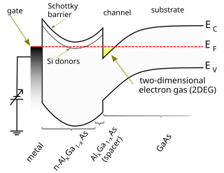
This article provides a more detailed explanation of p–n diode behavior than is found in the articles p–n junction or diode.

<span class="mw-page-title-main">Field effect (semiconductor)</span>

In physics, the field effect refers to the modulation of the electrical conductivity of a material by the application of an external electric field.

<span class="mw-page-title-main">Field-effect transistor</span> Type of transistor

The field-effect transistor (FET) is a type of transistor that uses an electric field to control the flow of current in a semiconductor. It comes in two types: junction FET (JFET) and metal-oxide-semiconductor FET (MOSFET). FETs have three terminals: source, gate, and drain. FETs control the flow of current by the application of a voltage to the gate, which in turn alters the conductivity between the drain and source.
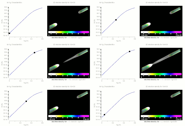
Electroreflectance is the change of reflectivity of a solid due to the influence of an electric field close to, or at the interface of the solid with a liquid. The change in reflectivity is most noticeable at very specific ranges of photon energy, corresponding to the band gaps at critical points of the Brillouin zone.

References

  1. 1 2 3 Zhang, Zhen; Yates, John T. (10 October 2012). "Band Bending in Semiconductors: Chemical and Physical Consequences at Surfaces and Interfaces". Chemical Reviews. 112 (10): 5520–5551. doi:10.1021/cr3000626. PMID   22783915.
  2. Just, Th. (April 1938). "G. W. Steller". Die Naturwissenschaften. 26 (14): 224. Bibcode:1938NW.....26..224J. doi:10.1007/BF01590290. S2CID   33381617.
  3. Mott, N. F. (October 1938). "Note on the contact between a metal and an insulator or semi-conductor". Mathematical Proceedings of the Cambridge Philosophical Society. 34 (4): 568–572. Bibcode:1938PCPS...34..568M. doi:10.1017/S0305004100020570. S2CID   222602877.
  4. Brillson, L. J. (2010). Surfaces and interfaces of electronic materials. Weinheim. ISBN   978-3527665723.{{cite book}}: CS1 maint: location missing publisher (link)
  5. 1 2 Jiang, Chaoran; Moniz, Savio J. A.; Wang, Aiqin; Zhang, Tao; Tang, Junwang (2017). "Photoelectrochemical devices for solar water splitting – materials and challenges" (PDF). Chemical Society Reviews. 46 (15): 4645–4660. doi: 10.1039/C6CS00306K . PMID   28644493.
  6. 1 2 Skromme, B.J. (2003). "Junctions and Barriers". Encyclopedia of Materials: Science and Technology: 1–12. doi:10.1016/B0-08-043152-6/01896-9. ISBN   9780080431529.
  7. Podrzaj, P.; Regojevic, B.; Kariz, Z. (February 2005). "An Enhanced Mechanical System for Studying the Basics of Control System Dynamics". IEEE Transactions on Education. 48 (1): 23–28. Bibcode:2005ITEdu..48...23P. doi:10.1109/TE.2004.825928. S2CID   571150.
  8. Griffiths, David J. (2017). Introduction to electrodynamics (Fourth ed.). Cambridge, United Kingdom. ISBN   978-1-108-42041-9.{{cite book}}: CS1 maint: location missing publisher (link)
  9. Veena, Misra; Öztürk, Mehmet C. (2005). The Electrical Engineering Handbook. Cambridge Massachusetts, United States: Academic Press. p. 109-126. ISBN   9780121709600.
  10. Lehovec, K. (15 August 1948). "The Photo-Voltaic Effect". Physical Review. 74 (4): 463–471. Bibcode:1948PhRv...74..463L. doi:10.1103/PhysRev.74.463.
  11. Schroder, Dieter K. (2001). "Surface voltage and surface photovoltage: history, theory and applications". Meas. Sci. Technol. 12 (3): R16–R31. Bibcode:2001MeScT..12R..16S. doi:10.1088/0957-0233/12/3/202. S2CID   250913018.
  12. Hüfner, Stefan, ed. (2007). Very High Resolution Photoelectron Spectroscopy. Lecture Notes in Physics. Vol. 715. Berlin, Heidelberg: Springer Berlin Heidelberg. doi:10.1007/3-540-68133-7. ISBN   978-3-540-68130-4.(subscription required)