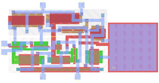
Photolithography is a process used in the manufacturing of integrated circuits. It involves using light to transfer a pattern onto a substrate, typically a silicon wafer.

Semiconductor device fabrication is the process used to manufacture semiconductor devices, typically integrated circuits (ICs) such as computer processors, microcontrollers, and memory chips that are present in everyday electrical and electronic devices. It is a multiple-step photolithographic and physio-chemical process during which electronic circuits are gradually created on a wafer, typically made of pure single-crystal semiconducting material. Silicon is almost always used, but various compound semiconductors are used for specialized applications.
In electronics and photonics design, tape-out or tapeout is the final result of the design process for integrated circuits or printed circuit boards before they are sent for manufacturing. The tapeout is specifically the point at which the graphic for the photomask of the circuit is sent to the fabrication facility.

In electronics, a wafer is a thin slice of semiconductor, such as a crystalline silicon (c-Si), used for the fabrication of integrated circuits and, in photovoltaics, to manufacture solar cells. The wafer serves as the substrate for microelectronic devices built in and upon the wafer. It undergoes many microfabrication processes, such as doping, ion implantation, etching, thin-film deposition of various materials, and photolithographic patterning. Finally, the individual microcircuits are separated by wafer dicing and packaged as an integrated circuit.

An application-specific integrated circuit is an integrated circuit (IC) chip customized for a particular use, rather than intended for general-purpose use, such as a chip designed to run in a digital voice recorder or a high-efficiency video codec. Application-specific standard product chips are intermediate between ASICs and industry standard integrated circuits like the 7400 series or the 4000 series. ASIC chips are typically fabricated using metal–oxide–semiconductor (MOS) technology, as MOS integrated circuit chips.
Electronic design automation (EDA), also referred to as electronic computer-aided design (ECAD), is a category of software tools for designing electronic systems such as integrated circuits and printed circuit boards. The tools work together in a design flow that chip designers use to design and analyze entire semiconductor chips. Since a modern semiconductor chip can have billions of components, EDA tools are essential for their design; this article in particular describes EDA specifically with respect to integrated circuits (ICs).

A photomask is an opaque plate with transparent areas that allow light to shine through in a defined pattern. Photomasks are commonly used in photolithography for the production of integrated circuits to produce a pattern on a thin wafer of material.
Wafer fabrication is a procedure composed of many repeated sequential processes to produce complete electrical or photonic circuits on semiconductor wafers in semiconductor device fabrication process. Examples include production of radio frequency (RF) amplifiers, LEDs, optical computer components, and microprocessors for computers. Wafer fabrication is used to build components with the necessary electrical structures.

A stepper is a device used in the manufacture of integrated circuits (ICs). It is an essential part of the process of photolithography, which creates millions of microscopic circuit elements on the surface of silicon wafers out of which chips are made. It is similar in operation to a slide projector or a photographic enlarger. The ICs that are made form the heart of computer processors, memory chips, and many other electronic devices.

The front-end-of-line (FEOL) is the first portion of IC fabrication where the individual components are patterned in the semiconductor. FEOL generally covers everything up to the deposition of metal interconnect layers.

Integrated circuit design, or IC design, is a sub-field of electronics engineering, encompassing the particular logic and circuit design techniques required to design integrated circuits, or ICs. ICs consist of miniaturized electronic components built into an electrical network on a monolithic semiconductor substrate by photolithography.

Microfabrication is the process of fabricating miniature structures of micrometre scales and smaller. Historically, the earliest microfabrication processes were used for integrated circuit fabrication, also known as "semiconductor manufacturing" or "semiconductor device fabrication". In the last two decades microelectromechanical systems (MEMS), microsystems, micromachines and their subfields, microfluidics/lab-on-a-chip, optical MEMS, RF MEMS, PowerMEMS, BioMEMS and their extension into nanoscale have re-used, adapted or extended microfabrication methods. Flat-panel displays and solar cells are also using similar techniques.
FOUP is a specialized plastic carrier designed to hold silicon wafers securely and safely in a controlled environment, and to allow the wafers to be transferred between machines for processing or measurement.
onsemi is an American semiconductor supplier company, based in Scottsdale, Arizona and ranked No. 483 on the 2022 Fortune 500 based on its 2021 sales. Products include power and signal management, logic, discrete, and custom devices for automotive, communications, computing, consumer, industrial, LED lighting, medical, military/aerospace and power applications. onsemi runs a network of manufacturing facilities, sales offices and design centers in North America, Europe, and the Asia Pacific regions. Based on its 2016 revenues of $3.907 billion, onsemi ranked among the worldwide top 20 semiconductor sales leaders.
Entegris, Inc. is an American provider of products and systems that purify, protect, and transport critical materials used in the semiconductor device fabrication process.
ASM is a Dutch headquartered multinational corporation that specializes in the design, manufacturing, sales and service of semiconductor wafer processing equipment for the fabrication of semiconductor devices. ASM's products are used by semiconductor manufacturers in front-end wafer processing in their semiconductor fabrication plants. ASM’s technologies include atomic layer deposition, epitaxy, chemical vapor deposition and diffusion.
GlobalFoundries Inc. (GF) is a multinational semiconductor contract manufacturing and design company incorporated in the Cayman Islands and headquartered in Malta, New York. Created by the divestiture of the manufacturing arm of AMD, the company was privately owned by Mubadala Investment Company, a sovereign wealth fund of the United Arab Emirates, until an initial public offering (IPO) in October 2021.
The SECS/GEM is the semiconductor's equipment interface protocol for equipment-to-host data communications. In an automated fab, the interface can start and stop equipment processing, collect measurement data, change variables and select recipes for products. The SECS /GEM standards do all this in a defined way.
In microtechnology, mask inspection or photomask inspection is an operation of checking the correctness of the fabricated photomasks, used, e.g., for semiconductor device fabrication.
Glossary of microelectronics manufacturing terms


