Scanning probe microscopy

Last updated

Scanning probe microscopy (SPM) is a branch of microscopy that forms images of surfaces using a physical probe that scans the specimen. SPM was founded in 1981, with the invention of the scanning tunneling microscope, an instrument for imaging surfaces at the atomic level. The first successful scanning tunneling microscope experiment was done by Gerd Binnig and Heinrich Rohrer. The key to their success was using a feedback loop to regulate gap distance between the sample and the probe. [1]

Contents

Many scanning probe microscopes can image several interactions simultaneously. The manner of using these interactions to obtain an image is generally called a mode.

The resolution varies somewhat from technique to technique, but some probe techniques reach a rather impressive atomic resolution.[ citation needed ] This is due largely because piezoelectric actuators can execute motions with a precision and accuracy at the atomic level or better on electronic command. This family of techniques can be called "piezoelectric techniques". The other common denominator is that the data are typically obtained as a two-dimensional grid of data points, visualized in false color as a computer image.

Established types

Image formation

To form images, scanning probe microscopes raster scan the tip over the surface. At discrete points in the raster scan a value is recorded (which value depends on the type of SPM and the mode of operation, see below). These recorded values are displayed as a heat map to produce the final STM images, usually using a black and white or an orange color scale.

Constant interaction mode

In constant interaction mode (often referred to as "in feedback"), a feedback loop is used to physically move the probe closer to or further from the surface (in the z axis) under study to maintain a constant interaction. This interaction depends on the type of SPM, for scanning tunneling microscopy the interaction is the tunnel current, for contact mode AFM or MFM it is the cantilever deflection, etc. The type of feedback loop used is usually a PI-loop, which is a PID-loop where the differential gain has been set to zero (as it amplifies noise). The z position of the tip (scanning plane is the xy-plane) is recorded periodically and displayed as a heat map. This is normally referred to as a topography image.

In this mode a second image, known as the ″error signal" or "error image" is also taken, which is a heat map of the interaction which was fed back on. Under perfect operation this image would be a blank at a constant value which was set on the feedback loop. Under real operation the image shows noise and often some indication of the surface structure. The user can use this image to edit the feedback gains to minimise features in the error signal.

If the gains are set incorrectly, many imaging artifacts are possible. If gains are too low features can appear smeared. If the gains are too high the feedback can become unstable and oscillate, producing striped features in the images which are not physical.

Constant height mode

In constant height mode the probe is not moved in the z-axis during the raster scan. Instead the value of the interaction under study is recorded (i.e. the tunnel current for STM, or the cantilever oscillation amplitude for amplitude modulated non-contact AFM). This recorded information is displayed as a heat map, and is usually referred to as a constant height image.

Constant height imaging is much more difficult than constant interaction imaging as the probe is much more likely to crash into the sample surface.[ citation needed ] Usually before performing constant height imaging one must image in constant interaction mode to check the surface has no large contaminants in the imaging region, to measure and correct for the sample tilt, and (especially for slow scans) to measure and correct for thermal drift of the sample. Piezoelectric creep can also be a problem, so the microscope often needs time to settle after large movements before constant height imaging can be performed.

Constant height imaging can be advantageous for eliminating the possibility of feedback artifacts.[ citation needed ]

Probe tips

The nature of an SPM probe tip depends entirely on the type of SPM being used. The combination of tip shape and topography of the sample make up a SPM image. [37] [ citation needed ] However, certain characteristics are common to all, or at least most, SPMs.[ citation needed ]

Most importantly the probe must have a very sharp apex.[ citation needed ] The apex of the probe defines the resolution of the microscope, the sharper the probe the better the resolution. For atomic resolution imaging the probe must be terminated by a single atom.[ citation needed ]

For many cantilever based SPMs (e.g. AFM and MFM), the entire cantilever and integrated probe are fabricated by acid [etching], [38] usually from silicon nitride. Conducting probes, needed for STM and SCM among others, are usually constructed from platinum/iridium wire for ambient operations, or tungsten for UHV operation. Other materials such as gold are sometimes used either for sample specific reasons or if the SPM is to be combined with other experiments such as TERS. Platinum/iridium (and other ambient) probes are normally cut using sharp wire cutters, the optimal method is to cut most of the way through the wire and then pull to snap the last of the wire, increasing the likelihood of a single atom termination. Tungsten wires are usually electrochemically etched, following this the oxide layer normally needs to be removed once the tip is in UHV conditions.

It is not uncommon for SPM probes (both purchased and "home-made") to not image with the desired resolution. This could be a tip which is too blunt or the probe may have more than one peak, resulting in a doubled or ghost image. For some probes, in situ modification of the tip apex is possible, this is usually done by either crashing the tip into the surface or by applying a large electric field. The latter is achieved by applying a bias voltage (of order 10V) between the tip and the sample, as this distance is usually 1-3 Angstroms, a very large field is generated.

The additional attachment of a quantum dot to the tip apex of a conductive probe enables surface potential imaging with high lateral resolution, scanning quantum dot microscopy.

Advantages

The resolution of the microscopes is not limited by diffraction, only by the size of the probe-sample interaction volume (i.e., point spread function), which can be as small as a few picometres. Hence the ability to measure small local differences in object height (like that of 135 picometre steps on <100> silicon) is unparalleled. Laterally the probe-sample interaction extends only across the tip atom or atoms involved in the interaction.

The interaction can be used to modify the sample to create small structures (Scanning probe lithography).

Unlike electron microscope methods, specimens do not require a partial vacuum but can be observed in air at standard temperature and pressure or while submerged in a liquid reaction vessel.

Disadvantages

The detailed shape of the scanning tip is sometimes difficult to determine. Its effect on the resulting data is particularly noticeable if the specimen varies greatly in height over lateral distances of 10 nm or less.

The scanning techniques are generally slower in acquiring images, due to the scanning process. As a result, efforts are being made to greatly improve the scanning rate. Like all scanning techniques, the embedding of spatial information into a time sequence opens the door to uncertainties in metrology, say of lateral spacings and angles, which arise due to time-domain effects like specimen drift, feedback loop oscillation, and mechanical vibration.

The maximum image size is generally smaller.

Scanning probe microscopy is often not useful for examining buried solid-solid or liquid-liquid interfaces.

Scanning photo current microscopy (SPCM)

SPCM can be considered as a member of the Scanning Probe Microscopy (SPM) family. The difference between other SPM techniques and SPCM is, it exploits a focused laser beam as the local excitation source instead of a probe tip. [39]

Characterization and analysis of spatially resolved optical behavior of materials is very important in opto-electronic industry. Simply this involves studying how the properties of a material vary across its surface or bulk structure. Techniques that enable spatially resolved optoelectronic measurements provide valuable insights for the enhancement of optical performance. Scanning electron microscopy (SPCM) has emerged as a powerful technique which can investigate spatially resolved optoelectronic properties in semiconductor nano structures.

Principle

Laser scan of the scanning photocurrent microscope Laser scan of the scanning photocurrent microscope.png
Laser scan of the scanning photocurrent microscope

In SPCM, a focused laser beam is used to excite the semiconducting material producing excitons (electro-hole pairs). These excitons undergo different mechanisms and if they can reach the nearby electrodes before the recombination takes place a photocurrent is generated. This photocurrent is position dependent as it, raster scans the device.

SPCM analysis

Using the position dependent photocurrent map, important photocurrent dynamics can be analyzed.

SPCM provides information such as characteristic length such as minority diffusion length, recombination dynamics, doping concentration, internal electric field  etc.

Visualization and analysis software

In all instances and contrary to optical microscopes, rendering software is necessary to produce images. Such software is produced and embedded by instrument manufacturers but also available as an accessory from specialized work groups or companies. The main packages used are freeware: Gwyddion, WSxM (developed by Nanotec) and commercial: SPIP (developed by Image Metrology), FemtoScan Online (developed by Advanced Technologies Center), MountainsMap SPM (developed by Digital Surf), TopoStitch (developed by Image Metrology).

Related Research Articles

<span class="mw-page-title-main">Scanning tunneling microscope</span> Instrument able to image surfaces at the atomic level by exploiting quantum tunneling effects

A scanning tunneling microscope (STM) is a type of scanning probe microscope used for imaging surfaces at the atomic level. Its development in 1981 earned its inventors, Gerd Binnig and Heinrich Rohrer, then at IBM Zürich, the Nobel Prize in Physics in 1986. STM senses the surface by using an extremely sharp conducting tip that can distinguish features smaller than 0.1 nm with a 0.01 nm (10 pm) depth resolution. This means that individual atoms can routinely be imaged and manipulated. Most scanning tunneling microscopes are built for use in ultra-high vacuum at temperatures approaching absolute zero, but variants exist for studies in air, water and other environments, and for temperatures over 1000 °C.

<span class="mw-page-title-main">Atomic force microscopy</span> Type of microscopy

Atomic force microscopy (AFM) or scanning force microscopy (SFM) is a very-high-resolution type of scanning probe microscopy (SPM), with demonstrated resolution on the order of fractions of a nanometer, more than 1000 times better than the optical diffraction limit.

Nanotribology is the branch of tribology that studies friction, wear, adhesion and lubrication phenomena at the nanoscale, where atomic interactions and quantum effects are not negligible. The aim of this discipline is characterizing and modifying surfaces for both scientific and technological purposes.

<span class="mw-page-title-main">Near-field scanning optical microscope</span>

Near-field scanning optical microscopy (NSOM) or scanning near-field optical microscopy (SNOM) is a microscopy technique for nanostructure investigation that breaks the far field resolution limit by exploiting the properties of evanescent waves. In SNOM, the excitation laser light is focused through an aperture with a diameter smaller than the excitation wavelength, resulting in an evanescent field on the far side of the aperture. When the sample is scanned at a small distance below the aperture, the optical resolution of transmitted or reflected light is limited only by the diameter of the aperture. In particular, lateral resolution of 6 nm and vertical resolution of 2–5 nm have been demonstrated.

Scanning probe lithography (SPL) describes a set of nanolithographic methods to pattern material on the nanoscale using scanning probes. It is a direct-write, mask-less approach which bypasses the diffraction limit and can reach resolutions below 10 nm. It is considered an alternative lithographic technology often used in academic and research environments. The term scanning probe lithography was coined after the first patterning experiments with scanning probe microscopes (SPM) in the late 1980s.

Scanning capacitance microscopy (SCM) is a variety of scanning probe microscopy in which a narrow probe electrode is positioned in contact or close proximity of a sample's surface and scanned. SCM characterizes the surface of the sample using information obtained from the change in electrostatic capacitance between the surface and the probe.

<span class="mw-page-title-main">Local oxidation nanolithography</span>

Local oxidation nanolithography (LON) is a tip-based nanofabrication method. It is based on the spatial confinement on an oxidation reaction under the sharp tip of an atomic force microscope.

A recurrence tracking microscope (RTM) is a microscope that is based on the quantum recurrence phenomenon of an atomic wave packet. It is used to investigate the nano-structure on a surface.
<span class="mw-page-title-main">Conductive atomic force microscopy</span> Method of measuring the microscopic topography of a material

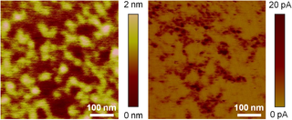
In microscopy, conductive atomic force microscopy (C-AFM) or current sensing atomic force microscopy (CS-AFM) is a mode in atomic force microscopy (AFM) that simultaneously measures the topography of a material and the electric current flow at the contact point of the tip with the surface of the sample. The topography is measured by detecting the deflection of the cantilever using an optical system, while the current is detected using a current-to-voltage preamplifier. The fact that the CAFM uses two different detection systems is a strong advantage compared to scanning tunneling microscopy (STM). Basically, in STM the topography picture is constructed based on the current flowing between the tip and the sample. Therefore, when a portion of a sample is scanned with an STM, it is not possible to discern if the current fluctuations are related to a change in the topography or to a change in the sample conductivity.

<span class="mw-page-title-main">Piezoresponse force microscopy</span> Microscopy technique for piezoelectric materials

Piezoresponse force microscopy (PFM) is a variant of atomic force microscopy (AFM) that allows imaging and manipulation of piezoelectric/ferroelectric materials domains. This is achieved by bringing a sharp conductive probe into contact with a ferroelectric surface and applying an alternating current (AC) bias to the probe tip in order to excite deformation of the sample through the converse piezoelectric effect (CPE). The resulting deflection of the probe cantilever is detected through standard split photodiode detector methods and then demodulated by use of a lock-in amplifier (LiA). In this way topography and ferroelectric domains can be imaged simultaneously with high resolution.

<span class="mw-page-title-main">Thermal scanning probe lithography</span>

Thermal scanning probe lithography (t-SPL) is a form of scanning probe lithography (SPL) whereby material is structured on the nanoscale using scanning probes, primarily through the application of thermal energy.

<span class="mw-page-title-main">Photoconductive atomic force microscopy</span> Type of atomic force microscopy

Photoconductive atomic force microscopy (PC-AFM) is a variant of atomic force microscopy that measures photoconductivity in addition to surface forces.

The technique of vibrational analysis with scanning probe microscopy allows probing vibrational properties of materials at the submicrometer scale, and even of individual molecules. This is accomplished by integrating scanning probe microscopy (SPM) and vibrational spectroscopy. This combination allows for much higher spatial resolution than can be achieved with conventional Raman/FTIR instrumentation. The technique is also nondestructive, requires non-extensive sample preparation, and provides more contrast such as intensity contrast, polarization contrast and wavelength contrast, as well as providing specific chemical information and topography images simultaneously.

<span class="mw-page-title-main">NanoWorld</span>

NanoWorld is the global market leader for tips for scanning probe microscopy (SPM) and atomic force microscopy (AFM). The atomic force microscope (AFM) is the defining instrument for the whole field of nanoscience and nanotechnology. It enables its users in research and high-tech industry to investigate materials at the atomic scale. AFM probes are the key consumable, the “finger” that enables the scientist to scan surfaces point-by-point at the atomic scale. Consistent high quality of the scanning probes is vital for reproducible results.

Nanosensors Inc. is a company that manufactures probes for use in atomic force microscopes (AFM) and scanning probe microscopes (SPM). This private, for profit company was founded November 21, 2018. Nanosensors Inc. is located in Neuchatel, Switzerland.

<span class="mw-page-title-main">Atomic force acoustic microscopy</span>

Atomic force acoustic microscopy (AFAM) is a type of scanning probe microscopy (SPM). It is a combination of acoustics and atomic force microscopy. The principal difference between AFAM and other forms of SPM is the addition of a transducer at the bottom of the sample which induces longitudinal out-of-plane vibrations in the specimen. These vibrations are sensed by a cantilever and tip called a probe. The figure shown here is the clear schematic of AFAM principle here B is the magnified version of the tip and sample placed on the transducer and tip having some optical coating generally gold coating to reflect the laser light on to the photodiode.

<span class="mw-page-title-main">Non-contact atomic force microscopy</span>

Non-contact atomic force microscopy (nc-AFM), also known as dynamic force microscopy (DFM), is a mode of atomic force microscopy, which itself is a type of scanning probe microscopy. In nc-AFM a sharp probe is moved close to the surface under study, the probe is then raster scanned across the surface, the image is then constructed from the force interactions during the scan. The probe is connected to a resonator, usually a silicon cantilever or a quartz crystal resonator. During measurements the sensor is driven so that it oscillates. The force interactions are measured either by measuring the change in amplitude of the oscillation at a constant frequency just off resonance or by measuring the change in resonant frequency directly using a feedback circuit to always drive the sensor on resonance.

The operation of a photon scanning tunneling microscope (PSTM) is analogous to the operation of an electron scanning tunneling microscope, with the primary distinction being that PSTM involves tunneling of photons instead of electrons from the sample surface to the probe tip. A beam of light is focused on a prism at an angle greater than the critical angle of the refractive medium in order to induce total internal reflection within the prism. Although the beam of light is not propagated through the surface of the refractive prism under total internal reflection, an evanescent field of light is still present at the surface.

A probe tip is an instrument used in scanning probe microscopes (SPMs) to scan the surface of a sample and make nano-scale images of surfaces and structures. The probe tip is mounted on the end of a cantilever and can be as sharp as a single atom. In microscopy, probe tip geometry and the composition of both the tip and the surface being probed directly affect resolution and imaging quality. Tip size and shape are extremely important in monitoring and detecting interactions between surfaces. SPMs can precisely measure electrostatic forces, magnetic forces, chemical bonding, Van der Waals forces, and capillary forces. SPMs can also reveal the morphology and topography of a surface.

Bimodal Atomic Force Microscopy is an advanced atomic force microscopy technique characterized by generating high-spatial resolution maps of material properties. Topography, deformation, elastic modulus, viscosity coefficient or magnetic field maps might be generated. Bimodal AFM is based on the simultaneous excitation and detection of two eigenmodes (resonances) of a force microscope microcantilever.

References

  1. Salapaka SM, Salapaka MV (2008). "Scanning Probe Microscopy". IEEE Control Systems Magazine. 28 (2): 65–83. doi:10.1109/MCS.2007.914688. ISSN   0272-1708. S2CID   20484280.
  2. Binnig G, Quate CF, Gerber C (March 1986). "Atomic force microscope". Physical Review Letters. 56 (9): 930–933. Bibcode:1986PhRvL..56..930B. doi: 10.1103/PhysRevLett.56.930 . PMID   10033323.
  3. Zhang L, Sakai T, Sakuma N, Ono T, Nakayama K (1999). "Nanostructural conductivity and surface-potential study of low-field-emission carbon films with conductive scanning probe microscopy". Applied Physics Letters. 75 (22): 3527–3529. Bibcode:1999ApPhL..75.3527Z. doi:10.1063/1.125377.
  4. Weaver JM, Abraham DW (1991). "High resolution atomic force microscopy potentiometry". Journal of Vacuum Science and Technology B. 9 (3): 1559–1561. Bibcode:1991JVSTB...9.1559W. doi:10.1116/1.585423.
  5. Nonnenmacher M, O'Boyle MP, Wickramasinghe HK (1991). "Kelvin probe force microscopy". Applied Physics Letters. 58 (25): 2921–2923. Bibcode:1991ApPhL..58.2921N. doi:10.1063/1.105227.
  6. Hartmann U (1988). "Magnetic force microscopy: Some remarks from the micromagnetic point of view". Journal of Applied Physics. 64 (3): 1561–1564. Bibcode:1988JAP....64.1561H. doi:10.1063/1.341836.
  7. Roelofs A, Böttger U, Waser R, Schlaphof F, Trogisch S, Eng LM (2000). "Differentiating 180° and 90° switching of ferroelectric domains with three-dimensional piezoresponse force microscopy". Applied Physics Letters. 77 (21): 3444–3446. Bibcode:2000ApPhL..77.3444R. doi:10.1063/1.1328049.
  8. Matey JR, Blanc J (1985). "Scanning capacitance microscopy". Journal of Applied Physics. 57 (5): 1437–1444. Bibcode:1985JAP....57.1437M. doi:10.1063/1.334506.
  9. Eriksson MA, Beck RG, Topinka M, Katine JA, Westervelt RM, Campman KL, et al. (July 29, 1996). "Cryogenic scanning probe characterization of semiconductor nanostructures". Applied Physics Letters. 69 (5): 671–673. Bibcode:1996ApPhL..69..671E. doi: 10.1063/1.117801 .
  10. Wagner C, Green MF, Leinen P, Deilmann T, Krüger P, Rohlfing M, et al. (July 2015). "Scanning Quantum Dot Microscopy". Physical Review Letters. 115 (2): 026101. arXiv: 1503.07738 . Bibcode:2015PhRvL.115b6101W. doi:10.1103/PhysRevLett.115.026101. PMID   26207484. S2CID   1720328.
  11. Trenkler T, De Wolf P, Vandervorst W, Hellemans L (1998). "Nanopotentiometry: Local potential measurements in complementary metal--oxide--semiconductor transistors using atomic force microscopy". Journal of Vacuum Science and Technology B. 16 (1): 367–372. Bibcode:1998JVSTB..16..367T. doi:10.1116/1.589812.
  12. Fritz M, Radmacher M, Petersen N, Gaub HE (May 1994). "Visualization and identification of intracellular structures by force modulation microscopy and drug induced degradation". The 1993 international conference on scanning tunneling microscopy. The 1993 international conference on scanning tunneling microscopy. Vol. 12. Beijing, China: AVS. pp. 1526–1529. Bibcode:1994JVSTB..12.1526F. doi: 10.1116/1.587278 . Archived from the original on March 5, 2016. Retrieved October 5, 2009.
  13. Luria J, Kutes Y, Moore A, Zhang L, Stach EA, Huey BD (September 26, 2016). "Charge transport in CdTe solar cells revealed by conductive tomographic atomic force microscopy". Nature Energy. 1 (11): 16150. Bibcode:2016NatEn...116150L. doi:10.1038/nenergy.2016.150. ISSN   2058-7546. OSTI   1361263. S2CID   138664678.
  14. Steffes JJ, Ristau RA, Ramesh R, Huey BD (February 2019). "Thickness scaling of ferroelectricity in BiFeO3 by tomographic atomic force microscopy". Proceedings of the National Academy of Sciences of the United States of America. 116 (7): 2413–2418. Bibcode:2019PNAS..116.2413S. doi: 10.1073/pnas.1806074116 . PMC   6377454 . PMID   30683718.
  15. Song J, Zhou Y, Huey BD (February 2021). "3D structure–property correlations of electronic and energy materials by tomographic atomic force microscopy". Applied Physics Letters. 118 (8). Bibcode:2021ApPhL.118h0501S. doi:10.1063/5.0040984. S2CID   233931111 . Retrieved March 11, 2024.
  16. Binnig G, Rohrer H, Gerber C, Weibel E (1982). "Tunneling through a controllable vacuum gap". Applied Physics Letters. 40 (2): 178–180. Bibcode:1982ApPhL..40..178B. doi: 10.1063/1.92999 .
  17. Kaiser WJ, Bell LD (April 1988). "Direct investigation of subsurface interface electronic structure by ballistic-electron-emission microscopy". Physical Review Letters. 60 (14): 1406–1409. Bibcode:1988PhRvL..60.1406K. doi:10.1103/PhysRevLett.60.1406. PMID   10038030.
  18. Higgins SR, Hamers RJ (March 1996). "Morphology and dissolution processes of metal sulfide minerals observed with the electrochemical scanning tunneling microscope". Journal of Vacuum Science and Technology B. 14 (2). AVS: 1360–1364. Bibcode:1996JVSTB..14.1360H. doi:10.1116/1.589098. Archived from the original on March 5, 2016. Retrieved October 5, 2009.
  19. Chang AM, Hallen HD, Harriott L, Hess HF, Kao HL, Kwo J, et al. (1992). "Scanning Hall probe microscopy". Applied Physics Letters. 61 (16): 1974–1976. Bibcode:1992ApPhL..61.1974C. doi:10.1063/1.108334. S2CID   121741603.
  20. Wiesendanger R, Bode M (July 25, 2001). "Nano- and atomic-scale magnetism studied by spin-polarized scanning tunneling microscopy and spectroscopy". Solid State Communications. 119 (4–5): 341–355. Bibcode:2001SSCom.119..341W. doi:10.1016/S0038-1098(01)00103-X. ISSN   0038-1098.
  21. Reddick RC, Warmack RJ, Ferrell TL (January 1989). "New form of scanning optical microscopy". Physical Review B. 39 (1): 767–770. Bibcode:1989PhRvB..39..767R. doi:10.1103/PhysRevB.39.767. PMID   9947227.
  22. Vorlesungsskript Physikalische Elektronik und Messtechnik (in German)
  23. Volker R, Freeland JF, Streiffer SK (2011). "New Capabilities at the Interface of X-Rays and Scanning Tunneling Microscopy". In Kalinin, Sergei V., Gruverman, Alexei (eds.). Scanning Probe Microscopy of Functional Materials: Nanoscale Imaging and Spectroscopy (1st ed.). New York: Springer. pp.  405–431. doi:10.1007/978-1-4419-7167-8_14. ISBN   978-1-4419-6567-7.
  24. Hansma PK, Drake B, Marti O, Gould SA, Prater CB (February 1989). "The scanning ion-conductance microscope". Science. 243 (4891): 641–643. Bibcode:1989Sci...243..641H. doi:10.1126/science.2464851. PMID   2464851.
  25. Meister A, Gabi M, Behr P, Studer P, Vörös J, Niedermann P, et al. (June 2009). "FluidFM: combining atomic force microscopy and nanofluidics in a universal liquid delivery system for single cell applications and beyond". Nano Letters. 9 (6): 2501–2507. Bibcode:2009NanoL...9.2501M. doi:10.1021/nl901384x. PMID   19453133.
  26. Sidles JA, Garbini JL, Bruland KJ, Rugar D, Züger O, Hoen S, et al. (1995). "Magnetic resonance force microscopy". Reviews of Modern Physics. 67 (1): 249–265. Bibcode:1995RvMP...67..249S. doi:10.1103/RevModPhys.67.249.
  27. Betzig E, Trautman JK, Harris TD, Weiner JS, Kostelak RL (March 1991). "Breaking the diffraction barrier: optical microscopy on a nanometric scale". Science. 251 (5000): 1468–1470. Bibcode:1991Sci...251.1468B. doi:10.1126/science.251.5000.1468. PMID   17779440. S2CID   6906302.
  28. Huth F, Govyadinov A, Amarie S, Nuansing W, Keilmann F, Hillenbrand R (August 2012). "Nano-FTIR absorption spectroscopy of molecular fingerprints at 20 nm spatial resolution". Nano Letters. 12 (8): 3973–3978. Bibcode:2012NanoL..12.3973H. doi:10.1021/nl301159v. PMID   22703339.
  29. De Wolf P, Snauwaert J, Clarysse T, Vandervorst W, Hellemans L (1995). "Characterization of a point-contact on silicon using force microscopy-supported resistance measurements". Applied Physics Letters. 66 (12): 1530–1532. Bibcode:1995ApPhL..66.1530D. doi:10.1063/1.113636.
  30. Xu JB, Lauger L, Dransfeld K, Wilson IH (1994). "Thermal sensors for investigation of heat transfer in scanning probe microscopy". Review of Scientific Instruments. 65 (7): 2262–2266. Bibcode:1994RScI...65.2262X. doi:10.1063/1.1145225.
  31. Yoo MJ, Fulton TA, Hess HF, Willett RL, Dunkleberger LN, Chichester RJ, et al. (April 1997). "Scanning Single-Electron Transistor Microscopy: Imaging Individual Charges". Science. 276 (5312): 579–582. doi:10.1126/science.276.5312.579. PMID   9110974.
  32. Nasr Esfahani E, Eshghinejad A, Ou Y, Zhao J, Adler S, Li J (November 2017). "Scanning Thermo-Ionic Microscopy: Probing Nanoscale Electrochemistry via Thermal Stress-Induced Oscillation". Microscopy Today. 25 (6): 12–19. arXiv: 1703.06184 . doi:10.1017/s1551929517001043. ISSN   1551-9295. S2CID   119463679.
  33. Eshghinejad A, Nasr Esfahani E, Wang P, Xie S, Geary TC, Adler SB, et al. (May 28, 2016). "Scanning thermo-ionic microscopy for probing local electrochemistry at the nanoscale". Journal of Applied Physics. 119 (20): 205110. Bibcode:2016JAP...119t5110E. doi:10.1063/1.4949473. ISSN   0021-8979. S2CID   7415218.
  34. Hong S, Tong S, Park WI, Hiranaga Y, Cho Y, Roelofs A (May 2014). "Charge gradient microscopy". Proceedings of the National Academy of Sciences of the United States of America. 111 (18): 6566–6569. Bibcode:2014PNAS..111.6566H. doi: 10.1073/pnas.1324178111 . PMC   4020115 . PMID   24760831.
  35. Esfahani EN, Liu X, Li J (2017). "Imaging ferroelectric domains via charge gradient microscopy enhanced by principal component analysis". Journal of Materiomics. 3 (4): 280–285. arXiv: 1706.02345 . doi:10.1016/j.jmat.2017.07.001. S2CID   118953680.
  36. Park H, Jung J, Min DK, Kim S, Hong S, Shin H (March 2, 2004). "Scanning resistive probe microscopy: Imaging ferroelectric domains". Applied Physics Letters. 84 (10): 1734–1736. Bibcode:2004ApPhL..84.1734P. doi:10.1063/1.1667266. ISSN   0003-6951.
  37. Bottomley LA (May 19, 1998). "Scanning Probe Microscopy". Analytical Chemistry. 70 (12): 425–476. doi:10.1021/a1980011o.
  38. Akamine S, Barrett RC, Quate CF (1990). "Improved atomic force microscope images using microcantilevers with sharp tips". Applied Physics Letters. 57 (3): 316–318. Bibcode:1990ApPhL..57..316A. doi:10.1063/1.103677.
  39. GRAHAM R, YU D (September 23, 2013). "SCANNING PHOTOCURRENT MICROSCOPY IN SEMICONDUCTOR NANOSTRUCTURES". Modern Physics Letters B. 27 (25): 1330018. doi:10.1142/s0217984913300184. ISSN   0217-9849.

Further reading