Related Research Articles
In electrical engineering, a ground plane is an electrically conductive surface, usually connected to electrical ground.

A printed circuit board is a medium used in electrical and electronic engineering to connect electronic components to one another in a controlled manner. It takes the form of a laminated sandwich structure of conductive and insulating layers: each of the conductive layers is designed with an artwork pattern of traces, planes and other features etched from one or more sheet layers of copper laminated onto and/or between sheet layers of a non-conductive substrate. Electrical components may be fixed to conductive pads on the outer layers in the shape designed to accept the component's terminals, generally by means of soldering, to both electrically connect and mechanically fasten them to it. Another manufacturing process adds vias: plated-through holes that allow interconnections between layers.

In electronics, point-to-point construction is a non-automated technique for constructing circuits which was widely used before the use of printed circuit boards (PCBs) and automated assembly gradually became widespread following their introduction in the 1950s. Circuits using thermionic valves were relatively large, relatively simple, and used large sockets, all of which made the PCB less obviously advantageous than with later complex semiconductor circuits. Point-to-point construction is still widespread in power electronics, where components are bulky and serviceability is a consideration, and to construct prototype equipment with few or heavy electronic components. A common practice, especially in older point-to-point construction, is to use the leads of components such as resistors and capacitors to bridge as much of the distance between connections as possible, reducing the need to add additional wire between the components.

A breadboard, solderless breadboard, or protoboard is a construction base used to build semi-permanent prototypes of electronic circuits. Unlike a perfboard or stripboard, breadboards do not require soldering or destruction of tracks and are hence reusable. For this reason, breadboards are also popular with students and in technological education.

Surface-mount technology (SMT), originally called planar mounting, is a method in which the electrical components are mounted directly onto the surface of a printed circuit board (PCB). An electrical component mounted in this manner is referred to as a surface-mount device (SMD). In industry, this approach has largely replaced the through-hole technology construction method of fitting components, in large part because SMT allows for increased manufacturing automation which reduces cost and improves quality. It also allows for more components to fit on a given area of substrate. Both technologies can be used on the same board, with the through-hole technology often used for components not suitable for surface mounting such as large transformers and heat-sinked power semiconductors.

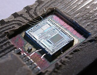
In electronics manufacturing, integrated circuit packaging is the final stage of semiconductor device fabrication, in which the block of semiconductor material is encapsulated in a supporting case that prevents physical damage and corrosion. The case, known as a "package", supports the electrical contacts which connect the device to a circuit board.

Printed circuit board milling is the process of removing areas of copper from a sheet of printed circuit board material to recreate the pads, signal traces and structures according to patterns from a digital circuit board plan known as a layout file. Similar to the more common and well known chemical PCB etch process, the PCB milling process is subtractive: material is removed to create the electrical isolation and ground planes required. However, unlike the chemical etch process, PCB milling is typically a non-chemical process and as such it can be completed in a typical office or lab environment without exposure to hazardous chemicals. High quality circuit boards can be produced using either process. In the case of PCB milling, the quality of a circuit board is chiefly determined by the system's true, or weighted, milling accuracy and control as well as the condition of the milling bits and their respective feed/rotational speeds. By contrast, in the chemical etch process, the quality of a circuit board depends on the accuracy and/or quality of the mask used to protect the copper from the chemicals and the state of the etching chemicals.

Differential signalling is a method for electrically transmitting information using two complementary signals. The technique sends the same electrical signal as a differential pair of signals, each in its own conductor. The pair of conductors can be wires in a twisted-pair or ribbon cable or traces on a printed circuit board.

In electronics, through-hole technology is a manufacturing scheme in which leads on the components are inserted through holes drilled in printed circuit boards (PCB) and soldered to pads on the opposite side, either by manual assembly or by the use of automated insertion mount machines.
A via is an electrical connection between copper layers in a printed circuit board. Essentially a via is a small drilled hole that goes through two or more adjacent layers; the hole is plated with copper that forms electrical connection through the insulation that separates the copper layers.

OrCAD Systems Corporation was a software company that made OrCAD, a proprietary software tool suite used primarily for electronic design automation (EDA). The software is used mainly by electronic design engineers and electronic technicians to create electronic schematics, and perform mixed-signal simulation and electronic prints for manufacturing printed circuit boards (PCBs). OrCAD was taken over by Cadence Design Systems in 1999 and was integrated with Cadence Allegro in 2005.

Signal integrity or SI is a set of measures of the quality of an electrical signal. In digital electronics, a stream of binary values is represented by a voltage waveform. However, digital signals are fundamentally analog in nature, and all signals are subject to effects such as noise, distortion, and loss. Over short distances and at low bit rates, a simple conductor can transmit this with sufficient fidelity. At high bit rates and over longer distances or through various mediums, various effects can degrade the electrical signal to the point where errors occur and the system or device fails. Signal integrity engineering is the task of analyzing and mitigating these effects. It is an important activity at all levels of electronics packaging and assembly, from internal connections of an integrated circuit (IC), through the package, the printed circuit board (PCB), the backplane, and inter-system connections. While there are some common themes at these various levels, there are also practical considerations, in particular the interconnect flight time versus the bit period, that cause substantial differences in the approach to signal integrity for on-chip connections versus chip-to-chip connections.

In electronics, the term copper pour refers to an area on a printed circuit board filled with copper. Copper pour is commonly used to create a ground plane. Another reason for using copper pour is to reduce the amount of etching fluid used during manufacturing.
An electronic circuit is composed of individual electronic components, such as resistors, transistors, capacitors, inductors and diodes, connected by conductive wires or traces through which electric current can flow. It is a type of electrical circuit and to be referred to as electronic, rather than electrical, generally at least one active component must be present. The combination of components and wires allows various simple and complex operations to be performed: signals can be amplified, computations can be performed, and data can be moved from one place to another.
Solder mask, solder stop mask or solder resist is a thin lacquer-like layer of polymer that is usually applied to the copper traces of a printed circuit board (PCB) for protection against oxidation and to prevent solder bridges from forming between closely spaced solder pads. A solder bridge is an unintended electrical connection between two conductors by means of a small blob of solder. PCBs use solder masks to prevent this from happening. Solder mask is not always used for hand soldered assemblies, but is essential for mass-produced boards that are soldered automatically using reflow or wave soldering techniques. Once applied, openings must be made in the solder mask wherever components are soldered, which is accomplished using photolithography. Solder mask is traditionally green, but is also available in many other colors.
In-circuit testing (ICT) is an example of white box testing where an electrical probe tests a populated printed circuit board (PCB), checking for shorts, opens, resistance, capacitance, and other basic quantities which will show whether the assembly was correctly fabricated. It may be performed with a "bed of nails" test fixture and specialist test equipment, or with a fixtureless in-circuit test setup.
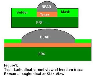
Bead probe technology (BPT) is technique used to provide electrical access to printed circuit board (PCB) circuitry for performing in-circuit testing (ICT). It makes use of small beads of solder placed onto the board's traces to allow measuring and controlling of the signals using a test probe. This permits test access to boards on which standard ICT test pads are not feasible due to space constraints.

DipTrace is a software suite for electronic design automation (EDA) to create schematic diagrams and printed circuit board layouts. DipTrace has four modules: schematic capture editor, PCB layout editor with built-in shape-based autorouter and 3D preview, component editor, and pattern editor.
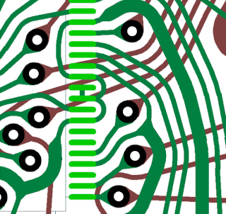
In printed circuit boards, teardrops are typically drop-shaped features at the junction of vias or contact pads and traces.
Specctra is a commercial PCB auto-router originally developed by John F. Cooper and David Chyan of Cooper & Chyan Technology, Inc. (CCT) in 1989. The company and product were taken over by Cadence Design Systems in May 1997. Since its integration into Cadence's Allegro PCB Editor, the name of the router is Allegro PCB Router. The latest version is 17.4 - 22.1.
References
- ↑ Watanabe, Tetsushi; Fujihara, Hiroshi; Wada, Osami; Koga, Ryuji; Kami, Yoshio (2004-08-01). "A Prediction Method of Common-Mode Excitation on a Printed Circuit Board Having a Signal Trace near the Ground Edge". IEICE Transactions on Communications. E87-B (8): 2327–2334. ISSN 0916-8516.
- ↑ Nawazi, Farwah (2022-04-25). "Signal Traces Parameters on Printed Circuit Board (PCB)". Circuits DIY. Retrieved 2022-11-22.
| | This electronics-related article is a stub. You can help Wikipedia by expanding it. |