Last updated Schematic of a basic SET and its internal electrical components
A single-electron transistor (SET) is a sensitive electronic device based on the Coulomb blockade effect. In this device the electrons flow through a tunnel junction between source/drain to a quantum dot (conductive island). Moreover, the electrical potential of the island can be tuned by a third electrode, known as the gate, which is capacitively coupled to the island. The conductive island is sandwiched between two tunnel junctions[1] modeled by capacitors, and , and resistors, and , in parallel.
A new subfield of condensed matter physics began in 1977 when David Thouless pointed out that, when made small enough, the size of a conductor affects its electronic properties.[2] This was followed by mesoscopic physics research in the 1980s based on the submicron-size of systems investigated.[3] Thus began research related to the single-electron transistor.
The first single-electron transistor based on the phenomenon of Coulomb blockade was reported in 1986 by Soviet scientists K. K. Likharev[ru] and D. V. Averin.[4] A couple years later, T. Fulton and G. Dolan at Bell Labs in the US fabricated and demonstrated how such a device works.[5] In 1992 Marc A. Kastner demonstrated the importance of the energy levels of the quantum dot.[6] In the late 1990s and early 2000s, Russian physicists S. P. Gubin, V. V. Kolesov, E. S. Soldatov, A. S. Trifonov, V. V. Khanin, G. B. Khomutov, and S. A. Yakovenko were the first ones to demonstrate a molecule-based SET operational at room temperature.[7]
Relevance
The increasing relevance of the Internet of things and the healthcare applications give more relevant impact to the electronic device power consumption. For this purpose, ultra-low power consumption is one of the main research topics into the current electronics world. The amazing number of tiny computers used in the day-to-day world (e.g. mobile phones and home electronics) requires a significant power consumption level of the implemented devices. In this scenario, the SET has appeared as a suitable candidate to achieve this low power range with high level of device integration.
Applicable areas include: super-sensitive electrometers, single-electron spectroscopy, DC current standards, temperature standards, detection of infrared radiation, voltage state logics, charge state logics, programmable single-electron transistor logic.[8]
Device
Principle
Schematic diagram of a single-electron transistorLeft to right: energy levels of source, island and drain in a single-electron transistor for the blocking state (upper part) and transmitting state (lower part).
The SET has, like the FET, three electrodes: source, drain, and a gate. The main technological difference between the transistor types is in the channel concept. While the channel changes from insulated to conductive with applied gate voltage in the FET, the SET is always insulated. The source and drain are coupled through two tunnel junctions, separated by a metallic or semiconductor-based quantum nanodot (QD),[9] also known as the "island". The electrical potential of the QD can be tuned with the capacitively coupled gate electrode to alter the resistance, by applying a positive voltage the QD will change from blocking to non-blocking state and electrons will start tunnelling to the QD. This phenomenon is known as the Coulomb blockade.
The current, from source to drain follows Ohm's law when is applied, and it equals where the main contribution of the resistance, comes from the tunnelling effects when electrons move from source to QD, and from QD to drain. regulates the resistance of the QD, which regulates the current. This is the exact same behaviour as in regular FETs. However, when moving away from the macroscopic scale, the quantum effects will affect the current,
In the blocking state all lower energy levels are occupied at the QD and no unoccupied level is within tunnelling range of electrons originating from the source (green 1.). When an electron arrives at the QD (2.) in the non-blocking state it will fill the lowest available vacant energy level, which will raise the energy barrier of the QD, taking it out of tunnelling distance once again. The electron will continue to tunnel through the second tunnel junction (3.), after which it scatters inelastically and reaches the drain electrode Fermi level (4.).
The energy levels of the QD are evenly spaced with a separation of This gives rise to a self-capacitance of the island, defined as: To achieve the Coulomb blockade, three criteria need to be met:[10]
The bias voltage must be lower than the elementary charge divided by the self-capacitance of the island:
The thermal energy in the source contact plus the thermal energy in the island, i.e. must be below the charging energy: otherwise the electron will be able to pass the QD via thermal excitation.
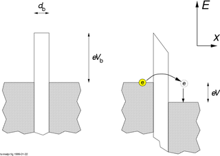
The tunnelling resistance, should be greater than which is derived from Heisenberg's uncertainty principle.[11] where corresponds to the tunnelling time and is shown as and in the schematic figure of the internal electrical components of the SET. The time () of electron tunnelling through the barrier is assumed to be negligibly small in comparison with the other time scales. This assumption is valid for tunnel barriers used in single-electron devices of practical interest, where
If the resistance of all the tunnel barriers of the system is much higher than the quantum resistance it is enough to confine the electrons to the island, and it is safe to ignore coherent quantum processes consisting of several simultaneous tunnelling events, i.e. co-tunnelling.
Theory
The background charge of the dielectric surrounding the QD is indicated by . and denote the number of electrons tunnelling through the two tunnel junctions and the total number of electrons is . The corresponding charges at the tunnel junctions can be written as:
where and are the parasitic leakage capacities of the tunnel junctions. Given the bias voltage, you can solve the voltages at the tunnel junctions:
The electrostatic energy of a double-connected tunnel junction (like the one in the schematical picture) will be
The work performed during electron tunnelling through the first and second transitions will be:
Given the standard definition of free energy in the form:
where we find the free energy of a SET as:
For further consideration, it is necessary to know the change in free energy at zero temperatures at both tunnel junctions:
The probability of a tunnel transition will be high when the change in free energy is negative. The main term in the expressions above determines a positive value of as long as the applied voltage will not exceed the threshold value, which depends on the smallest capacity in the system. In general, for an uncharged QD ( and ) for symmetric transitions () we have the condition
(that is, the threshold voltage is reduced by half compared with a single transition).
When the applied voltage is zero, the Fermi level at the metal electrodes will be inside the energy gap. When the voltage increases to the threshold value, tunnelling from left to right occurs, and when the reversed voltage increases above the threshold level, tunnelling from right to left occurs.
The existence of the Coulomb blockade is clearly visible in the current–voltage characteristic of a SET (a graph showing how the drain current depends on the gate voltage). At low gate voltages (in absolute value), the drain current will be zero, and when the voltage increases above the threshold, the transitions behave like an ohmic resistance (both transitions have the same permeability) and the current increases linearly. The background charge in a dielectric can not only reduce, but completely block the Coulomb blockade.
In the case where the permeability of the tunnel barriers is very different a stepwise I-V characteristic of the SET arises. An electron tunnels to the island through the first transition and is retained on it, due to the high tunnel resistance of the second transition. After a certain period of time, the electron tunnels through the second transition, however, this process causes a second electron to tunnel to the island through the first transition. Therefore, most of the time the island is charged in excess of one charge. For the case with the inverse dependence of permeability the island will be unpopulated and its charge will decrease stepwise.[citation needed] Only now can we understand the principle of operation of a SET. Its equivalent circuit can be represented as two tunnel junctions connected in series via the QD, perpendicular to the tunnel junctions is another control electrode (gate) connected. The gate electrode is connected to the island through a control tank The gate electrode can change the background charge in the dielectric, since the gate additionally polarizes the island so that the island charge becomes equal to
Substituting this value into the formulas found above, we find new values for the voltages at the transitions:
The electrostatic energy should include the energy stored on the gate capacitor, and the work performed by the voltage on the gate should be taken into account in the free energy:
At zero temperatures, only transitions with negative free energy are allowed: or . These conditions can be used to find areas of stability in the plane
With increasing voltage at the gate electrode, when the supply voltage is maintainted below the voltage of the Coulomb blockade (i.e. ), the drain output current will oscillate with a period These areas correspond to failures in the field of stability. The oscillations of the tunnelling current occur in time, and the oscillations in two series-connected junctions have a periodicity in the gate control voltage. The thermal broadening of the oscillations increases to a large extent with increasing temperature.
Temperature dependence
Various materials have successfully been tested when creating single-electron transistors. However, temperature is a huge factor limiting implementation in available electronical devices. Most of the metallic-based SETs only work at extremely low temperatures.
Single-electron transistor with niobium leads and aluminium island
As mentioned in bullet 2 in the list above: the electrostatic charging energy must be greater than to prevent thermal fluctuations affecting the Coulomb blockade. This in turn implies that the maximum allowed island capacitance is inversely proportional to the temperature, and needs to be below 1 aF to make the device operational at room temperature.
The island capacitance is a function of the QD size, and a QD diameter smaller than 10nm is preferable when aiming for operation at room temperature. This in turn puts huge restraints on the manufacturability of integrated circuits because of reproducibility issues.
CMOS compatibility
Hybrid SET–FET circuit
The level of the electrical current of the SET can be amplified enough to work with available CMOS technology by generating a hybrid SET–FET device.[12][13]
The EU funded, in 2016, project IONS4SET (#688072)[14] looks for the manufacturability of SET–FET circuits operative at room temperature. The main goal of this project is to design a SET-manufacturability process-flow for large-scale operations seeking to extend the use of the hybrid SET–CMOS architectures. To assure room temperature operation, single dots of diameters below 5nm have to be fabricated and located between source and drain with tunnel distances of a few nanometers.[15] Up to now there is no reliable process-flow to manufacture a hybrid SET–FET circuit operative at room temperature. In this context, this EU project explores a more feasible way to manufacture the SET–FET circuit by using pillar dimensions of approximately 10nm.[16]
A scanning tunneling microscope (STM) is a type of microscope used for imaging surfaces at the atomic level. Its development in 1981 earned its inventors, Gerd Binnig and Heinrich Rohrer, then at IBM Zürich, the Nobel Prize in Physics in 1986. STM senses the surface by using an extremely sharp conducting tip that can distinguish features smaller than 0.1 nm with a 0.01 nm (10 pm) depth resolution. This means that individual atoms can routinely be imaged and manipulated. Most scanning tunneling microscopes are built for use in ultra-high vacuum at temperatures approaching absolute zero, but variants exist for studies in air, water and other environments, and for temperatures over 1000 °C.
The metal–oxide–semiconductor field-effect transistor is a type of field-effect transistor (FET), most commonly fabricated by the controlled oxidation of silicon. It has an insulated gate, the voltage of which determines the conductivity of the device. This ability to change conductivity with the amount of applied voltage can be used for amplifying or switching electronic signals. The term metal–insulator–semiconductor field-effect transistor (MISFET) is almost synonymous with MOSFET. Another near-synonym is insulated-gate field-effect transistor (IGFET).
The junction field-effect transistor (JFET) is one of the simplest types of field-effect transistor. JFETs are three-terminal semiconductor devices that can be used as electronically controlled switches or resistors, or to build amplifiers.
A bipolar junction transistor (BJT) is a type of transistor that uses both electrons and electron holes as charge carriers. In contrast, a unipolar transistor, such as a field-effect transistor (FET), uses only one kind of charge carrier. A bipolar transistor allows a small current injected at one of its terminals to control a much larger current flowing between the terminals, making the device capable of amplification or switching.
A Langmuir probe is a device used to determine the electron temperature, electron density, and electric potential of a plasma. It works by inserting one or more electrodes into a plasma, with a constant or time-varying electric potential between the various electrodes or between them and the surrounding vessel. The measured currents and potentials in this system allow the determination of the physical properties of the plasma.
Capacitance is the capability of a material object or device to store electric charge. It is measured by the charge in response to a difference in electric potential, expressed as the ratio of those quantities. Commonly recognized are two closely related notions of capacitance: self capacitance and mutual capacitance. An object that can be electrically charged exhibits self capacitance, for which the electric potential is measured between the object and ground. Mutual capacitance is measured between two components, and is particularly important in the operation of the capacitor, an elementary linear electronic component designed to add capacitance to an electric circuit.
A Schottky barrier, named after Walter H. Schottky, is a potential energy barrier for electrons formed at a metal–semiconductor junction. Schottky barriers have rectifying characteristics, suitable for use as a diode. One of the primary characteristics of a Schottky barrier is the Schottky barrier height, denoted by ΦB. The value of ΦB depends on the combination of metal and semiconductor.
A p–n junction is a boundary or interface between two types of semiconductor materials, p-type and n-type, inside a single crystal of semiconductor. The "p" (positive) side contains an excess of holes, while the "n" (negative) side contains an excess of electrons in the outer shells of the electrically neutral atoms there. This allows electric current to pass through the junction only in one direction. The p- and n-type regions creating the junction are made by doping the semiconductor, for example by ion implantation, diffusion of dopants, or by epitaxy.
In solid-state physics, the electron mobility characterises how quickly an electron can move through a metal or semiconductor when pulled by an electric field. There is an analogous quantity for holes, called hole mobility. The term carrier mobility refers in general to both electron and hole mobility.
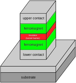
Tunnel magnetoresistance (TMR) is a magnetoresistive effect that occurs in a magnetic tunnel junction (MTJ), which is a component consisting of two ferromagnets separated by a thin insulator. If the insulating layer is thin enough, electrons can tunnel from one ferromagnet into the other. Since this process is forbidden in classical physics, the tunnel magnetoresistance is a strictly quantum mechanical phenomenon, and lies in the study of spintronics.
In quantum computing, a charge qubit is a qubit whose basis states are charge states. In superconducting quantum computing, a charge qubit is formed by a tiny superconducting island coupled by a Josephson junction to a superconducting reservoir. The state of the qubit is determined by the number of Cooper pairs that have tunneled across the junction. In contrast with the charge state of an atomic or molecular ion, the charge states of such an "island" involve a macroscopic number of conduction electrons of the island. The quantum superposition of charge states can be achieved by tuning the gate voltage U that controls the chemical potential of the island. The charge qubit is typically read-out by electrostatically coupling the island to an extremely sensitive electrometer such as the radio-frequency single-electron transistor.
The threshold voltage, commonly abbreviated as Vth or VGS(th), of a field-effect transistor (FET) is the minimum gate-to-source voltage (VGS) that is needed to create a conducting path between the source and drain terminals. It is an important scaling factor to maintain power efficiency.
Diffusion Capacitance is the capacitance that happens due to transport of charge carriers between two terminals of a device, for example, the diffusion of carriers from anode to cathode in a forward biased diode or from emitter to base in a forward-biased junction of a transistor. In a semiconductor device with a current flowing through it at a particular moment there is necessarily some charge in the process of transit through the device. If the applied voltage changes to a different value and the current changes to a different value, a different amount of charge will be in transit in the new circumstances. The change in the amount of transiting charge divided by the change in the voltage causing it is the diffusion capacitance. The adjective "diffusion" is used because the original use of this term was for junction diodes, where the charge transport was via the diffusion mechanism. See Fick's laws of diffusion.
In semiconductor physics, the depletion region, also called depletion layer, depletion zone, junction region, space charge region, or space charge layer, is an insulating region within a conductive, doped semiconductor material where the mobile charge carriers have diffused away, or forced away by an electric field. The only elements left in the depletion region are ionized donor or acceptor impurities. This region of uncovered positive and negative ions is called the depletion region due to the depletion of carriers in this region, leaving none to carry a current. Understanding the depletion region is key to explaining modern semiconductor electronics: diodes, bipolar junction transistors, field-effect transistors, and variable capacitance diodes all rely on depletion region phenomena.
In mesoscopic physics, a Coulomb blockade (CB), named after Charles-Augustin de Coulomb's electrical force, is the decrease in electrical conductance at small bias voltages of a small electronic device comprising at least one low-capacitance tunnel junction. Because of the CB, the conductance of a device may not be constant at low bias voltages, but disappear for biases under a certain threshold, i.e. no current flows.
The Shockley diode equation, or the diode law, named after transistor co-inventor William Shockley of Bell Labs, models the exponential current–voltage (I–V) relationship of semiconductor diodes in moderate constant current forward bias or reverse bias:
In quantum computing, and more specifically in superconducting quantum computing, the phase qubit is a superconducting device based on the superconductor–insulator–superconductor (SIS) Josephson junction, designed to operate as a quantum bit, or qubit.
A carbon nanotube field-effect transistor (CNTFET) is a field-effect transistor that utilizes a single carbon nanotube (CNT) or an array of carbon nanotubes as the channel material, instead of bulk silicon, as in the traditional MOSFET structure. There have been major developments since CNTFETs were first demonstrated in 1998.
Single-walled carbon nanotubes in the fields of quantum mechanics and nanoelectronics, have the ability to conduct electricity. This conduction can be ballistic, diffusive, or based on scattering. When ballistic in nature conductance can be treated as if the electrons experience no scattering.
This article provides a more detailed explanation of p–n diode behavior than is found in the articles p–n junction or diode.
↑ Gubin, S. P.; Gulayev, Yu V.; Khomutov, G. B.; Kislov, V. V.; Kolesov, V. V.; Soldatov, E. S.; Sulaimankulov, K. S.; Trifonov, A. S. (2002). "Molecular clusters as building blocks for nanoelectronics: the first demonstration of a cluster single-electron tunnelling transistor at room temperature". Nanotechnology. 13 (2): 185–194. Bibcode:2002Nanot..13..185G. doi:10.1088/0957-4484/13/2/311..
↑ Klupfel, F. J.; Burenkov, A.; Lorenz, J. (2016). "Simulation of silicon-dot-based single-electron memory devices". 2016 International Conference on Simulation of Semiconductor Processes and Devices (SISPAD). pp.237–240. doi:10.1109/SISPAD.2016.7605191. ISBN978-1-5090-0818-6. S2CID15721282.
↑ Xu, Xiaomo; Heinig, Karl-Heinz; Möller, Wolfhard; Engelmann, Hans-Jürgen; Klingner, Nico; Gharbi, Ahmed; Tiron, Raluca; Johannes von Borany; Hlawacek, Gregor (2019). "Morphology modification of Si nanopillars under ion irradiation at elevated temperatures: Plastic deformation and controlled thinning to 10 nm". arXiv:1906.09975v2 [physics.app-ph].
This page is based on this Wikipedia article Text is available under the CC BY-SA 4.0 license; additional terms may apply. Images, videos and audio are available under their respective licenses.