
The Hall effect is the production of a potential difference across an electrical conductor that is transverse to an electric current in the conductor and to an applied magnetic field perpendicular to the current. It was discovered by Edwin Hall in 1879.
Magnetoresistance is the tendency of a material to change the value of its electrical resistance in an externally-applied magnetic field. There are a variety of effects that can be called magnetoresistance. Some occur in bulk non-magnetic metals and semiconductors, such as geometrical magnetoresistance, Shubnikov–de Haas oscillations, or the common positive magnetoresistance in metals. Other effects occur in magnetic metals, such as negative magnetoresistance in ferromagnets or anisotropic magnetoresistance (AMR). Finally, in multicomponent or multilayer systems, giant magnetoresistance (GMR), tunnel magnetoresistance (TMR), colossal magnetoresistance (CMR), and extraordinary magnetoresistance (EMR) can be observed.
Spintronics, also known as spin electronics, is the study of the intrinsic spin of the electron and its associated magnetic moment, in addition to its fundamental electronic charge, in solid-state devices. The field of spintronics concerns spin-charge coupling in metallic systems; the analogous effects in insulators fall into the field of multiferroics.
In particle physics, spin polarization is the degree to which the spin, i.e., the intrinsic angular momentum of elementary particles, is aligned with a given direction. This property may pertain to the spin, hence to the magnetic moment, of conduction electrons in ferromagnetic metals, such as iron, giving rise to spin-polarized currents. It may refer to (static) spin waves, preferential correlation of spin orientation with ordered lattices.
Multiferroics are defined as materials that exhibit more than one of the primary ferroic properties in the same phase:
A two-dimensional electron gas (2DEG) is a scientific model in solid-state physics. It is an electron gas that is free to move in two dimensions, but tightly confined in the third. This tight confinement leads to quantized energy levels for motion in the third direction, which can then be ignored for most problems. Thus the electrons appear to be a 2D sheet embedded in a 3D world. The analogous construct of holes is called a two-dimensional hole gas (2DHG), and such systems have many useful and interesting properties.
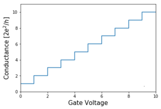
A quantum point contact (QPC) is a narrow constriction between two wide electrically conducting regions, of a width comparable to the electronic wavelength.
A charge density wave (CDW) is an ordered quantum fluid of electrons in a linear chain compound or layered crystal. The electrons within a CDW form a standing wave pattern and sometimes collectively carry an electric current. The electrons in such a CDW, like those in a superconductor, can flow through a linear chain compound en masse, in a highly correlated fashion. Unlike a superconductor, however, the electric CDW current often flows in a jerky fashion, much like water dripping from a faucet due to its electrostatic properties. In a CDW, the combined effects of pinning and electrostatic interactions likely play critical roles in the CDW current's jerky behavior, as discussed in sections 4 & 5 below.
The quantum spin Hall state is a state of matter proposed to exist in special, two-dimensional semiconductors that have a quantized spin-Hall conductance and a vanishing charge-Hall conductance. The quantum spin Hall state of matter is the cousin of the integer quantum Hall state, and that does not require the application of a large magnetic field. The quantum spin Hall state does not break charge conservation symmetry and spin- conservation symmetry.
Gallium manganese arsenide, chemical formula (Ga,Mn)As is a magnetic semiconductor. It is based on the world's second most commonly used semiconductor, gallium arsenide,, and readily compatible with existing semiconductor technologies. Differently from other dilute magnetic semiconductors, such as the majority of those based on II-VI semiconductors, it is not paramagnetic but ferromagnetic, and hence exhibits hysteretic magnetization behavior. This memory effect is of importance for the creation of persistent devices. In (Ga,Mn)As, the manganese atoms provide a magnetic moment, and each also acts as an acceptor, making it a p-type material. The presence of carriers allows the material to be used for spin-polarized currents. In contrast, many other ferromagnetic magnetic semiconductors are strongly insulating and so do not possess free carriers. (Ga,Mn)As is therefore a candidate as a spintronic material.

The nitrogen-vacancy center is one of numerous point defects in diamond. Its most explored and useful property is its photoluminescence, which allows observers to read out its spin-state. The NV center's electron spin, localized at atomic scales, can be manipulated at room temperature by external factors such as magnetic, or electric fields, microwave radiation, or optical light, resulting in sharp resonances in the intensity of the photoluminescence. These resonances can be explained in terms of electron spin related phenomena such as quantum entanglement, spin–orbit interaction and Rabi oscillations, and analysed using advanced quantum optics theory. An individual NV center can be used as a basic unit for a quantum computer, a qubit, and used for quantum cryptography. Further potential applications in novel fields of electronics and sensing include spintronics, masers, and quantum sensors. If the charge is not specified the term "NV center" refers to the negatively charged NV− center.
A composite fermion is the topological bound state of an electron and an even number of quantized vortices, sometimes visually pictured as the bound state of an electron and, attached, an even number of magnetic flux quanta. Composite fermions were originally envisioned in the context of the fractional quantum Hall effect, but subsequently took on a life of their own, exhibiting many other consequences and phenomena.
A trion is a localized excitation which consists of three charged particles. A negative trion consists of two electrons and one hole and a positive trion consists of two holes and one electron. The trion itself is a quasiparticle and is somewhat similar to an exciton, which is a complex of one electron and one hole. The trion has a ground singlet state (spin S = 1/2) and an excited triplet state (S = 3/2). Here singlet and triplet degeneracies originate not from the whole system but from the two identical particles in it. The half-integer spin value distinguishes trions from excitons in many phenomena; for example, energy states of trions, but not excitons, are split in an applied magnetic field. Trion states were predicted theoretically in 1958; they were observed experimentally in 1993 in CdTe/Cd1−xZnxTe quantum wells, and later in various other optically excited semiconductor structures. There are experimental proofs of their existence in nanotubes supported by theoretical studies. Despite numerous reports of experimental trion observations in different semiconductor heterostructures, there are serious concerns on the exact physical nature of the detected complexes. The originally foreseen 'true' trion particle has a delocalized wavefunction (at least at the scales of several Bohr radii) while recent studies reveal significant binding from charged impurities in real semiconductor quantum wells.
In quantum mechanics, orbital magnetization, Morb, refers to the magnetization induced by orbital motion of charged particles, usually electrons in solids. The term "orbital" distinguishes it from the contribution of spin degrees of freedom, Mspin, to the total magnetization. A nonzero orbital magnetization requires broken time-reversal symmetry, which can occur spontaneously in ferromagnetic and ferrimagnetic materials, or can be induced in a non-magnetic material by an applied magnetic field.
The Aharonov–Casher effect is a quantum mechanical phenomenon predicted in 1984 by Yakir Aharonov and Aharon Casher, in which a traveling magnetic dipole is affected by an electric field. It is dual to the Aharonov–Bohm effect, in which the quantum phase of a charged particle depends upon which side of a magnetic flux tube it comes through. In the Aharonov–Casher effect, the particle has a magnetic moment and the tubes are charged instead. It was observed in a gravitational neutron interferometer in 1989 and later by fluxon interference of magnetic vortices in Josephson junctions. It has also been seen with electrons and atoms.
Valleytronics is an experimental area in semiconductors that exploits local extrema ("valleys") in the electronic band structure. Certain semiconductors have multiple "valleys" in the electronic band structure of the first Brillouin zone, and are known as multivalley semiconductors. Valleytronics is the technology of control over the valley degree of freedom, a local maximum/minimum on the valence/conduction band, of such multivalley semiconductors.
Electric dipole spin resonance (EDSR) is a method to control the magnetic moments inside a material using quantum mechanical effects like the spin–orbit interaction. Mainly, EDSR allows to flip the orientation of the magnetic moments through the use of electromagnetic radiation at resonant frequencies. EDSR was first proposed by Emmanuel Rashba.
Graphene is a semimetal whose conduction and valence bands meet at the Dirac points, which are six locations in momentum space, the vertices of its hexagonal Brillouin zone, divided into two non-equivalent sets of three points. The two sets are labeled K and K'. The sets give graphene a valley degeneracy of gv = 2. By contrast, for traditional semiconductors the primary point of interest is generally Γ, where momentum is zero. Four electronic properties separate it from other condensed matter systems.
Spin Hall magnetoresistance (SMR) is a transport phenomenon that is found in some electrical conductors that have at least one surface in direct contact with another magnetic material due to changes in the spin current that are present in metals and semiconductors with a large spin Hall angle. It is most easily detected when the magnetic material is an insulator which eliminates other magnetically sensitive transport effects arising from conduction in the magnetic material.

The Rashba–Edelstein effect (REE) is a spintronics-related effect, consisting in the conversion of a bidimensional charge current into a spin accumulation. This effect is an intrinsic charge-to-spin conversion mechanism and it was predicted in 1990 by the scientist V.M. Edelstein. It has been demonstrated in 2013 and confirmed by several experimental evidences in the following years.

