Minimum source-to-gate voltage for a field effect transistor to be conducting from source to drain
Simulation result for formation of inversion channel (electron density) and attainment of threshold voltage (IV) in a nanowire MOSFET. Note that the y-axis is logarithmic, showing that only extremely small amounts of current pass below the threshold voltage (around 0.45V) when the conducting channel connects.
The threshold voltage, commonly abbreviated as Vth or VGS(th), of a field-effect transistor (FET) is the minimum gate-to-source voltage (VGS) that is needed to create a conducting path between the source and drain terminals. It is an important scaling factor to maintain power efficiency.
When referring to a junction field-effect transistor (JFET), the threshold voltage is often called pinch-off voltage instead.[1][2] This is somewhat confusing since pinch off applied to insulated-gate field-effect transistor (IGFET) refers to the channel pinching that leads to current saturation behaviour under high source–drain bias, even though the current is never off. Unlike pinch off, the term threshold voltage is unambiguous and refers to the same concept in any field-effect transistor.
Basic principles
In n-channelenhancement-mode devices, a conductive channel does not exist naturally within the transistor, and a positive gate-to-source voltage is necessary to create one such. The positive voltage attracts free-floating electrons within the body towards the gate, forming a conductive channel. But first, enough electrons must be attracted near the gate to counter the dopant ions added to the body of the FET; this forms a region with no mobile carriers called a depletion region, and the voltage at which this occurs is the threshold voltage of the FET. Further gate-to-source voltage increase will attract even more electrons towards the gate which are able to create a conductive channel from source to drain; this process is called inversion. The reverse is true for the p-channel "enhancement-mode" MOS transistor. When VGS = 0 the device is “OFF” and the channel is open / non-conducting. The application of a negative gate voltage to the p-type "enhancement-mode" MOSFET enhances the channels conductivity turning it “ON”.
In contrast, n-channel depletion-mode devices have a conductive channel naturally existing within the transistor. Accordingly, the term threshold voltage does not readily apply to turning such devices on, but is used instead to denote the voltage level at which the channel is wide enough to allow electrons to flow easily. This ease-of-flow threshold also applies to p-channeldepletion-mode devices, in which a negative voltage from gate to body/source creates a depletion layer by forcing the positively charged holes away from the gate-insulator/semiconductor interface, leaving exposed a carrier-free region of immobile, negatively charged acceptor ions.
For the n-channel depletion MOS transistor, a negative gate-source voltage will deplete (hence its name) the conductive channel of its free electrons switching the transistor “OFF”. Likewise for a p-channel "depletion-mode" MOS transistor a positive gate-source voltage will deplete the channel of its free holes, turning it “OFF”.
In wide planar transistors the threshold voltage is essentially independent of the drain–source voltage and is therefore a well defined characteristic, however it is less clear in modern nanometer-sized MOSFETs due to drain-induced barrier lowering.
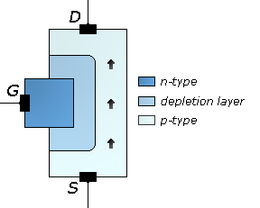
Depletion region of an enhancement-mode nMOSFET biased below the threshold
Depletion region of an enhancement-mode nMOSFET biased above the threshold with channel formed
In the figures, the source (left side) and drain (right side) are labeled n+ to indicate heavily doped (blue) n-regions. The depletion layer dopant is labeled NA− to indicate that the ions in the (pink) depletion layer are negatively charged and there are very few holes. In the (red) bulk the number of holes p=NA making the bulk charge neutral.
If the gate voltage is below the threshold voltage (left figure), the "enhancement-mode" transistor is turned off and ideally there is no current from the drain to the source of the transistor. In fact, there is a current even for gate biases below the threshold (subthreshold leakage) current, although it is small and varies exponentially with gate bias. Therefore, datasheets will specify threshold voltage according to a specified measurable amount of current (commonly 250 μA or 1 mA).
If the gate voltage is above the threshold voltage (right figure), the "enhancement-mode" transistor is turned on, due to there being many electrons in the channel at the oxide-silicon interface, creating a low-resistance channel where charge can flow from drain to source. For voltages significantly above the threshold, this situation is called strong inversion. The channel is tapered when VD > 0 because the voltage drop due to the current in the resistive channel reduces the oxide field supporting the channel as the drain is approached.
Body effect
The body effect is the change in the threshold voltage by an amount approximately equal to the change in the source-bulk voltage, , because the body influences the threshold voltage (when it is not tied to the source). It can be thought of as a second gate, and is sometimes referred to as the back gate, and accordingly the body effect is sometimes called the back-gate effect.[3]
For an enhancement-mode nMOS MOSFET, the body effect upon threshold voltage is computed according to the Shichman–Hodges model,[4] which is accurate for older process nodes,[clarification needed] using the following equation:
where is the threshold voltage when substrate bias is present, is the source-to-body substrate bias, is the surface potential, and is threshold voltage for zero substrate bias, is the body effect parameter, is oxide thickness, is oxide permittivity, is the permittivity of silicon, is a doping concentration, is elementary charge.
Dependence on oxide thickness
In a given technology node, such as the 90-nm CMOS process, the threshold voltage depends on the choice of oxide and on oxide thickness. Using the body formulas above, is directly proportional to , and , which is the parameter for oxide thickness.
Thus, the thinner the oxide thickness, the lower the threshold voltage. Although this may seem to be an improvement, it is not without cost; because the thinner the oxide thickness, the higher the subthreshold leakage current through the device will be. Consequently, the design specification for 90-nm gate-oxide thickness was set at 1nm to control the leakage current.[5] This kind of tunneling, called Fowler-Nordheim Tunneling.[6]
where and are constants and is the electric field across the gate oxide.
Before scaling the design features down to 90nm, a dual-oxide approach for creating the oxide thickness was a common solution to this issue. With a 90nmprocess technology, a triple-oxide approach has been adopted in some cases.[7] One standard thin oxide is used for most transistors, another for I/O driver cells, and a third for memory-and-pass transistor cells. These differences are based purely on the characteristics of oxide thickness on threshold voltage of CMOS technologies.
Temperature dependence
As with the case of oxide thickness affecting threshold voltage, temperature has an effect on the threshold voltage of a CMOS device. Expanding on part of the equation in the body effect section
where is half the contact potential, is the Boltzmann constant, is temperature, is the elementary charge, is a doping parameter and is the intrinsic doping parameter for the substrate.
We see that the surface potential has a direct relationship with the temperature. Looking above, that the threshold voltage does not have a direct relationship but is not independent of the effects. This variation is typically between −4mV/K and −2mV/K depending on doping level.[8] For a change of 30°C this results in significant variation from the 500mV design parameter commonly used for the 90-nm technology node.
Dependence on random dopant fluctuation
Random dopant fluctuation (RDF) is a form of process variation resulting from variation in the implanted impurity concentration. In MOSFET transistors, RDF in the channel region can alter the transistor's properties, especially threshold voltage. In newer process technologies RDF has a larger effect because the total number of dopants is fewer.[9]
Research works are being carried out in order to suppress the dopant fluctuation which leads to the variation of threshold voltage between devices undergoing same manufacturing process.[10]
A transistor is a semiconductor device used to amplify or switch electrical signals and power. The transistor is one of the basic building blocks of modern electronics. It is composed of semiconductor material, usually with at least three terminals for connection to an electronic circuit. A voltage or current applied to one pair of the transistor's terminals controls the current through another pair of terminals. Because the controlled (output) power can be higher than the controlling (input) power, a transistor can amplify a signal. Some transistors are packaged individually, but many more are found embedded in integrated circuits.
The metal–oxide–semiconductor field-effect transistor is a type of field-effect transistor (FET), most commonly fabricated by the controlled oxidation of silicon. It has an insulated gate, the voltage of which determines the conductivity of the device. This ability to change conductivity with the amount of applied voltage can be used for amplifying or switching electronic signals. A metal-insulator-semiconductor field-effect transistor (MISFET) is a term almost synonymous with MOSFET. Another synonym is IGFET for insulated-gate field-effect transistor.
The junction-gate field-effect transistor (JFET) is one of the simplest types of field-effect transistor. JFETs are three-terminal semiconductor devices that can be used as electronically controlled switches or resistors, or to build amplifiers.
Complementary metal–oxide–semiconductor is a type of metal–oxide–semiconductor field-effect transistor (MOSFET) fabrication process that uses complementary and symmetrical pairs of p-type and n-type MOSFETs for logic functions. CMOS technology is used for constructing integrated circuit (IC) chips, including microprocessors, microcontrollers, memory chips, and other digital logic circuits. CMOS technology is also used for analog circuits such as image sensors, data converters, RF circuits, and highly integrated transceivers for many types of communication.
A high-electron-mobility transistor (HEMT), also known as heterostructure FET (HFET) or modulation-doped FET (MODFET), is a field-effect transistor incorporating a junction between two materials with different band gaps as the channel instead of a doped region. A commonly used material combination is GaAs with AlGaAs, though there is wide variation, dependent on the application of the device. Devices incorporating more indium generally show better high-frequency performance, while in recent years, gallium nitride HEMTs have attracted attention due to their high-power performance. Like other FETs, HEMTs are used in integrated circuits as digital on-off switches. FETs can also be used as amplifiers for large amounts of current using a small voltage as a control signal. Both of these uses are made possible by the FET’s unique current–voltage characteristics. HEMT transistors are able to operate at higher frequencies than ordinary transistors, up to millimeter wave frequencies, and are used in high-frequency products such as cell phones, satellite television receivers, voltage converters, and radar equipment. They are widely used in satellite receivers, in low power amplifiers and in the defense industry.
The term high-κ dielectric refers to a material with a high dielectric constant, as compared to silicon dioxide. High-κ dielectrics are used in semiconductor manufacturing processes where they are usually used to replace a silicon dioxide gate dielectric or another dielectric layer of a device. The implementation of high-κ gate dielectrics is one of several strategies developed to allow further miniaturization of microelectronic components, colloquially referred to as extending Moore's Law. Sometimes these materials are called "high-k", instead of "high-κ".
A power MOSFET is a specific type of metal–oxide–semiconductor field-effect transistor (MOSFET) designed to handle significant power levels. Compared to the other power semiconductor devices, such as an insulated-gate bipolar transistor (IGBT) or a thyristor, its main advantages are high switching speed and good efficiency at low voltages. It shares with the IGBT an isolated gate that makes it easy to drive. They can be subject to low gain, sometimes to a degree that the gate voltage needs to be higher than the voltage under control.
Channel length modulation (CLM) is an effect in field effect transistors, a shortening of the length of the inverted channel region with increase in drain bias for large drain biases. The result of CLM is an increase in current with drain bias and a reduction of output resistance. It is one of several short-channel effects in MOSFET scaling. It also causes distortion in JFET amplifiers.
A VMOS transistor is a type of MOSFET. VMOS is also used for describing the V-groove shape vertically cut into the substrate material. VMOS is an acronym for "vertical metal oxide semiconductor", or "V-groove MOS".
Capacitance–voltage profiling is a technique for characterizing semiconductor materials and devices. The applied voltage is varied, and the capacitance is measured and plotted as a function of voltage. The technique uses a metal–semiconductor junction or a p–n junction or a MOSFET to create a depletion region, a region which is empty of conducting electrons and holes, but may contain ionized donors and electrically active defects or traps. The depletion region with its ionized charges inside behaves like a capacitor. By varying the voltage applied to the junction it is possible to vary the depletion width. The dependence of the depletion width upon the applied voltage provides information on the semiconductor's internal characteristics, such as its doping profile and electrically active defect densities., Measurements may be done at DC, or using both DC and a small-signal AC signal, or using a large-signal transient voltage.
Charge trap flash (CTF) is a semiconductor memory technology used in creating non-volatile NOR and NAND flash memory. It is a type of floating-gate MOSFET memory technology, but differs from the conventional floating-gate technology in that it uses a silicon nitride film to store electrons rather than the doped polycrystalline silicon typical of a floating-gate structure. This approach allows memory manufacturers to reduce manufacturing costs five ways:
Fewer process steps are required to form a charge storage node
Smaller process geometries can be used
Multiple bits can be stored on a single flash memory cell.
Improved reliability
Higher yield since the charge trap is less susceptible to point defects in the tunnel oxide layer
In semiconductor electronics fabrication technology, a self-aligned gate is a transistor manufacturing feature whereby the gate electrode of a MOSFET is used as a mask for the doping of the source and drain regions. This technique ensures that the gate is naturally and precisely aligned to the edges of the source and drain.
A multigate device, multi-gate MOSFET or multi-gate field-effect transistor (MuGFET) refers to a metal–oxide–semiconductor field-effect transistor (MOSFET) that has more than one gate on a single transistor. The multiple gates may be controlled by a single gate electrode, wherein the multiple gate surfaces act electrically as a single gate, or by independent gate electrodes. A multigate device employing independent gate electrodes is sometimes called a multiple-independent-gate field-effect transistor (MIGFET). The most widely used multi-gate devices are the FinFET and the GAAFET, which are non-planar transistors, or 3D transistors.
Drain-induced barrier lowering (DIBL) is a short-channel effect in MOSFETs referring originally to a reduction of threshold voltage of the transistor at higher drain voltages. In a classic planar field-effect transistor with a long channel, the bottleneck in channel formation occurs far enough from the drain contact that it is electrostatically shielded from the drain by the combination of the substrate and gate, and so classically the threshold voltage was independent of drain voltage. In short-channel devices this is no longer true: The drain is close enough to gate the channel, and so a high drain voltage can open the bottleneck and turn on the transistor prematurely.
Overdrive voltage, usually abbreviated as VOV, is typically referred to in the context of MOSFET transistors. The overdrive voltage is defined as the voltage between transistor gate and source (VGS) in excess of the threshold voltage (VTH) where VTH is defined as the minimum voltage required between gate and source to turn the transistor on. Due to this definition, overdrive voltage is also known as "excess gate voltage" or "effective voltage." Overdrive voltage can be found using the simple equation: VOV = VGS − VTH.
A metal gate, in the context of a lateral metal–oxide–semiconductor (MOS) stack, is the gate electrode separated by an oxide from the transistor's channel – the gate material is made from a metal. In most MOS transistors since about the mid 1970s, the "M" for metal has been replaced by a non-metal gate material.
The gate oxide is the dielectric layer that separates the gate terminal of a MOSFET from the underlying source and drain terminals as well as the conductive channel that connects source and drain when the transistor is turned on. Gate oxide is formed by thermal oxidation of the silicon of the channel to form a thin insulating layer of silicon dioxide. The insulating silicon dioxide layer is formed through a process of self-limiting oxidation, which is described by the Deal–Grove model. A conductive gate material is subsequently deposited over the gate oxide to form the transistor. The gate oxide serves as the dielectric layer so that the gate can sustain as high as 1 to 5 MV/cm transverse electric field in order to strongly modulate the conductance of the channel.
In field-effect transistors (FETs), depletion mode and enhancement mode are two major transistor types, corresponding to whether the transistor is in an on state or an off state at zero gate–source voltage.
Polysilicon depletion effect is the phenomenon in which unwanted variation of threshold voltage of the MOSFET devices using polysilicon as gate material is observed, leading to unpredicted behavior of the electronic circuit. Because of this variation High-k Dielectric Metal Gates (HKMG) were introduced to solve the issue.
The field-effect transistor (FET) is a type of transistor that uses an electric field to control the flow of current in a semiconductor. FETs are devices with three terminals: source, gate, and drain. FETs control the flow of current by the application of a voltage to the gate, which in turn alters the conductivity between the drain and source.
This page is based on this Wikipedia article Text is available under the CC BY-SA 4.0 license; additional terms may apply. Images, videos and audio are available under their respective licenses.