
A transistor is a semiconductor device used to amplify or switch electrical signals and power. It is one of the basic building blocks of modern electronics. It is composed of semiconductor material, usually with at least three terminals for connection to an electronic circuit. A voltage or current applied to one pair of the transistor's terminals controls the current through another pair of terminals. Because the controlled (output) power can be higher than the controlling (input) power, a transistor can amplify a signal. Some transistors are packaged individually, but many more in miniature form are found embedded in integrated circuits.

The metal-oxide-semiconductor field-effect transistor is a type of field-effect transistor (FET), most commonly fabricated by the controlled oxidation of silicon. It has an insulated gate, the voltage of which determines the conductivity of the device. This ability to change conductivity with the amount of applied voltage can be used for amplifying or switching electronic signals. A metal-insulator-semiconductor field-effect transistor (MISFET) is a term almost synonymous with MOSFET. Another synonym is IGFET for insulated-gate field-effect transistor.

The junction-gate field-effect transistor (JFET) is one of the simplest types of field-effect transistor. JFETs are three-terminal semiconductor devices that can be used as electronically controlled switches or resistors, or to build amplifiers.

In electronics, a comparator is a device that compares two voltages or currents and outputs a digital signal indicating which is larger. It has two analog input terminals and and one binary digital output . The output is ideally
N-type metal–oxide–semiconductor logic uses n-type (-) MOSFETs to implement logic gates and other digital circuits. These nMOS transistors operate by creating an inversion layer in a p-type transistor body. This inversion layer, called the n-channel, can conduct electrons between n-type "source" and "drain" terminals. The n-channel is created by applying voltage to the third terminal, called the gate. Like other MOSFETs, nMOS transistors have four modes of operation: cut-off, triode, saturation, and velocity saturation.

Complementary metal–oxide–semiconductor is a type of metal–oxide–semiconductor field-effect transistor (MOSFET) fabrication process that uses complementary and symmetrical pairs of p-type and n-type MOSFETs for logic functions. CMOS technology is used for constructing integrated circuit (IC) chips, including microprocessors, microcontrollers, memory chips, and other digital logic circuits. CMOS technology is also used for analog circuits such as image sensors, data converters, RF circuits, and highly integrated transceivers for many types of communication.
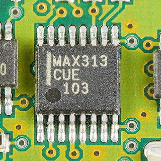
The analogueswitch, also called the bilateral switch, is an electronic component that behaves in a similar way to a relay, but has no moving parts. The switching element is normally a pair of MOSFET transistors, one an N-channel device, the other a P-channel device. The device can conduct analog or digital signals in either direction when on and isolates the switched terminals when off. Analogue switches are usually manufactured as integrated circuits in packages containing multiple switches. These include the 4016 and 4066 from the 4000 series.

A differential amplifier is a type of electronic amplifier that amplifies the difference between two input voltages but suppresses any voltage common to the two inputs. It is an analog circuit with two inputs and and one output , in which the output is ideally proportional to the difference between the two voltages:
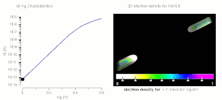
The threshold voltage, commonly abbreviated as Vth or VGS(th), of a field-effect transistor (FET) is the minimum gate-to-source voltage (VGS) that is needed to create a conducting path between the source and drain terminals. It is an important scaling factor to maintain power efficiency.

IC power-supply pins denote a voltage and current supply terminals in electric, electronics engineering, and in Integrated circuit design. Integrated circuits (ICs) have at least two pins that connect to the power rails of the circuit in which they are installed. These are known as the power-supply pins. However, the labeling of the pins varies by IC family and manufacturer. The double subscript notation usually corresponds to a first letter in a given IC family (transistors) notation of the terminals.
The cascode is a two-stage amplifier that consists of a common-emitter stage feeding into a common-base stage.
Diode logic constructs AND and OR logic gates with diodes and resistors.
Open collector output and open drain output utilize a transistor as a switch that either disconnects or connects an integrated circuit (IC) output pin to ground, instead of outputting a specific voltage or current.
The floating-gate MOSFET (FGMOS), also known as a floating-gate MOS transistor or floating-gate transistor, is a type of metal–oxide–semiconductor field-effect transistor (MOSFET) where the gate is electrically isolated, creating a floating node in direct current, and a number of secondary gates or inputs are deposited above the floating gate (FG) and are electrically isolated from it. These inputs are only capacitively connected to the FG. Since the FG is surrounded by highly resistive material, the charge contained in it remains unchanged for long periods of time, nowadays typically longer than 10 years. Usually Fowler-Nordheim tunneling and hot-carrier injection mechanisms are used to modify the amount of charge stored in the FG.
In the field of electronics, a technique where part of the output of a system is used at startup can be described as bootstrapping.
An electronic circuit is composed of individual electronic components, such as resistors, transistors, capacitors, inductors and diodes, connected by conductive wires or traces through which electric current can flow. It is a type of electrical circuit and to be referred to as electronic, rather than electrical, generally at least one active component must be present. The combination of components and wires allows various simple and complex operations to be performed: signals can be amplified, computations can be performed, and data can be moved from one place to another.
PMOS or pMOS logic is a family of digital circuits based on p-channel, enhancement mode metal–oxide–semiconductor field-effect transistors (MOSFETs). In the late 1960s and early 1970s, PMOS logic was the dominant semiconductor technology for large-scale integrated circuits before being superseded by NMOS and CMOS devices.
In electronics, pass transistor logic (PTL) describes several logic families used in the design of integrated circuits. It reduces the count of transistors used to make different logic gates, by eliminating redundant transistors. Transistors are used as switches to pass logic levels between nodes of a circuit, instead of as switches connected directly to supply voltages. This reduces the number of active devices, but has the disadvantage that the difference of the voltage between high and low logic levels decreases at each stage. Each transistor in series is less saturated at its output than at its input. If several devices are chained in series in a logic path, a conventionally constructed gate may be required to restore the signal voltage to the full value. By contrast, conventional CMOS logic switches transistors so the output connects to one of the power supply rails, so logic voltage levels in a sequential chain do not decrease. Simulation of circuits may be required to ensure adequate performance.

In field-effect transistors (FETs), depletion mode and enhancement mode are two major transistor types, corresponding to whether the transistor is in an on state or an off state at zero gate–source voltage.

The field-effect transistor (FET) is a type of transistor that uses an electric field to control the flow of current in a semiconductor. FETs are devices with three terminals: source, gate, and drain. FETs control the flow of current by the application of a voltage to the gate, which in turn alters the conductivity between the drain and source.


