Tungsten diselenide

Last updated
Tungsten diselenide
STM of WSe2 on HOPG.jpg
WSe2 monolayer on graphene (yellow) and its atomic image (inset) [1]
Molybdenite-3D-balls.png
Identifiers
3D model (JSmol)
ECHA InfoCard 100.031.877 OOjs UI icon edit-ltr-progressive.svg
EC Number
  • 235-078-7
PubChem CID
  • InChI=1S/2Se.W
    Key: ROUIDRHELGULJS-UHFFFAOYSA-N
  • [Se]=[W]=[Se]
Properties
WSe2
Molar mass 341.76 g/mol
Appearancegrey to black solid
Odor odorless
Density 9.32 g/cm3 [2]
Melting point > 1200 °C
insoluble
Band gap ~1 eV (indirect, bulk) [3]
~1.7 eV (direct, monolayer) [4]
Structure
hP6, space group P6
3
/mmc, No 194 [2]
a = 0.3297 nm, c = 1.2982 nm
Trigonal prismatic (WIV)
Pyramidal (Se2−)
Thermochemistry
-185.3 kJ mol−1 [5]
Hazards
Occupational safety and health (OHS/OSH):
Main hazards
External MSDS
Related compounds
Other anions
Tantalum diselenide
Except where otherwise noted, data are given for materials in their standard state (at 25 °C [77 °F], 100 kPa).

Tungsten diselenide is an inorganic compound with the formula WSe2. [6] The compound adopts a hexagonal crystalline structure similar to molybdenum disulfide. The tungsten atoms are covalently bonded to six selenium ligands in a trigonal prismatic coordination sphere while each selenium is bonded to three tungsten atoms in a pyramidal geometry. The tungsten–selenium bond has a length of 0.2526 nm, and the distance between selenium atoms is 0.334 nm. [7] It is a well studied example of a layered material. The layers stack together via van der Waals interactions. WSe2 is a very stable semiconductor in the group-VI transition metal dichalcogenides.

Contents

Structure and properties

The hexagonal (P63/mmc) polymorph 2H-WSe2 is isotypic with hexagonal MoS2. The two-dimensional lattice structure has W and Se arranged periodically in layers with hexagonal symmetry. Similar to graphite, van der Waals interactions hold the layers together; however, the 2D-layers in WSe2 are not atomically thin. The large size of the W cation renders the lattice structure of WSe2 more sensitive to changes than MoS2. [8]

In addition to the typical semiconducting hexagonal structure, a second metallic polymorph of WSe2 exists. This phasem 1T-WSe2, is based on a tetragonal symmetry with one WSe2 layer per repeating unit. The 1T-WSe2 phase is less stable and transitions to the 2H-WSe2 phase. [8] [9] WSe2 can form a fullerene-like structure.

The Young’s modulus vary greatly as a function of the number of layers in a flake. For a single monolayer, the reported Young’s modulus is 258.6 ± 38.3 GPa. [10]

Synthesis

Heating thin films of tungsten under pressure from gaseous selenium and high temperatures (>800 K) using the sputter deposition technique leads to the films crystallizing in hexagonal structures with the correct stoichiometric ratio. [11]

W + 2 Se → WSe2

Potential applications

Atomic image of a WSe2 monolayer showing hexagonal symmetry and three-fold defects. Scale bar: 2 nm (0.5 nm in the inset). WSe2 TEM.jpg
Atomic image of a WSe2 monolayer showing hexagonal symmetry and three-fold defects. Scale bar: 2 nm (0.5 nm in the inset).

The potential applications of transition metal dichalcogenides in solar cells and photonics are often discussed. [13] Bulk WSe
2
has an optical band gap of ~1.35 eV with a temperature dependence of −4.6×10⁻⁴ eV/K. [14] WSe
2
photoelectrodes are stable in both acidic and basic conditions, making them potentially useful in electrochemical solar cells. [15] [16] [17]

The properties of WSe
2
monolayers differ from those of the bulk state, as is typical for semiconductors. Mechanically exfoliated monolayers of WSe
2
are transparent photovoltaic materials with LED properties. [18] The resulting solar cells pass 95 percent of the incident light, with one tenth of the remaining five percent converted into electrical power. [19] [20] The material can be changed from p-type to n-type by changing the voltage of an adjacent metal electrode from positive to negative, allowing devices made from it to have tunable bandgaps. [21]

See also

Related Research Articles

<span class="mw-page-title-main">Molybdenum disulfide</span> Chemical compound

Molybdenum disulfide is an inorganic compound composed of molybdenum and sulfur. Its chemical formula is MoS
2
.

<span class="mw-page-title-main">Chalcogenide</span>

A chalcogenide is a chemical compound consisting of at least one chalcogen anion and at least one more electropositive element. Although all group 16 elements of the periodic table are defined as chalcogens, the term chalcogenide is more commonly reserved for sulfides, selenides, tellurides, and polonides, rather than oxides. Many metal ores exist as chalcogenides. Photoconductive chalcogenide glasses are used in xerography. Some pigments and catalysts are also based on chalcogenides. The metal dichalcogenide MoS2 is a common solid lubricant.

<span class="mw-page-title-main">Tungsten disulfide</span> Chemical compound

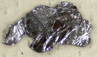
Tungsten disulfide is an inorganic chemical compound composed of tungsten and sulfur with the chemical formula WS2. This compound is part of the group of materials called the transition metal dichalcogenides. It occurs naturally as the rare mineral tungstenite. This material is a component of certain catalysts used for hydrodesulfurization and hydrodenitrification.

<span class="mw-page-title-main">Tungsten ditelluride</span> Chemical compound

Tungsten ditelluride (WTe2) is an inorganic semimetallic chemical compound. In October 2014, tungsten ditelluride was discovered to exhibit an extremely large magnetoresistance: 13 million percent resistance increase in a magnetic field of 60 tesla at 0.5 kelvin. The resistance is proportional to the square of the magnetic field and shows no saturation. This may be due to the material being the first example of a compensated semimetal, in which the number of mobile holes is the same as the number of electrons. Tungsten ditelluride has layered structure, similar to many other transition metal dichalcogenides, but its layers are so distorted that the honeycomb lattice many of them have in common is in WTe2 hard to recognize. The tungsten atoms instead form zigzag chains, which are thought to behave as one-dimensional conductors. Unlike electrons in other two-dimensional semiconductors, the electrons in WTe2 can easily move between the layers.

<span class="mw-page-title-main">Tantalum(IV) sulfide</span> Chemical compound

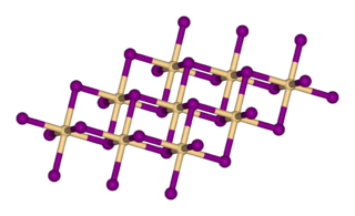
Tantalum(IV) sulfide is an inorganic compound with the formula TaS2. It is a layered compound with three-coordinate sulfide centres and trigonal prismatic or octahedral metal centres. It is structurally similar to molybdenum disulfide MoS2, and numerous other transition metal dichalcogenides. Tantalum disulfide has three polymorphs 1T-TaS2, 2H-TaS2, and 3R-TaS2, representing trigonal, hexagonal, and rhombohedral respectively.

A trion is a localized excitation which consists of three charged particles. A negative trion consists of two electrons and one hole and a positive trion consists of two holes and one electron. The trion itself is a quasiparticle and is somewhat similar to an exciton, which is a complex of one electron and one hole. The trion has a ground singlet state (spin S = 1/2) and an excited triplet state (S = 3/2). Here singlet and triplet degeneracies originate not from the whole system but from the two identical particles in it. The half-integer spin value distinguishes trions from excitons in many phenomena; for example, energy states of trions, but not excitons, are split in an applied magnetic field. Trion states were predicted theoretically in 1958; they were observed experimentally in 1993 in CdTe/Cd1−xZnxTe quantum wells, and later in various other optically excited semiconductor structures. There are experimental proofs of their existence in nanotubes supported by theoretical studies. Despite numerous reports of experimental trion observations in different semiconductor heterostructures, there are serious concerns on the exact physical nature of the detected complexes. The originally foreseen 'true' trion particle has a delocalized wavefunction (at least at the scales of several Bohr radii) while recent studies reveal significant binding from charged impurities in real semiconductor quantum wells.

Diselenide may refer to:

<span class="mw-page-title-main">Titanium disulfide</span> Inorganic chemical compound

Titanium disulfide is an inorganic compound with the formula TiS2. A golden yellow solid with high electrical conductivity, it belongs to a group of compounds called transition metal dichalcogenides, which consist of the stoichiometry ME2. TiS2 has been employed as a cathode material in rechargeable batteries.

Piezo-phototronic effect is a three-way coupling effect of piezoelectric, semiconductor and photonic properties in non-central symmetric semiconductor materials, using the piezoelectric potential (piezopotential) that is generated by applying a strain to a semiconductor with piezoelectricity to control the carrier generation, transport, separation and/or recombination at metal–semiconductor junction or p–n junction for improving the performance of optoelectronic devices, such as photodetector, solar cell and light-emitting diode. Prof. Zhong Lin Wang at Georgia Institute of Technology proposed the fundamental principle of this effect in 2010.

<span class="mw-page-title-main">Titanium diselenide</span> Chemical compound

Titanium diselenide (TiSe2) also known as titanium(IV) selenide, is an inorganic compound of titanium and selenium. In this material selenium is viewed as selenide (Se2−) which requires that titanium exists as Ti4+. Titanium diselenide is a member of metal dichalcogenides, compounds that consist of a metal and an element of the chalcogen column within the periodic table. Many exhibit properties of potential value in battery technology, such as intercalation and electrical conductivity, although most applications focus on the less toxic and lighter disulfides, e.g. TiS2.

<span class="mw-page-title-main">Molybdenum diselenide</span> Chemical compound

Molybdenum diselenide is an inorganic compound of molybdenum and selenium. Its structure is similar to that of MoS
2
. Compounds of this category are known as transition metal dichalcogenides, abbreviated TMDCs. These compounds, as the name suggests, are made up of a transition metals and elements of group 16 on the periodic table of the elements. Compared to MoS
2
, MoSe
2
exhibits higher electrical conductivity.

<span class="mw-page-title-main">Transition metal dichalcogenide monolayers</span> Thin semiconductors

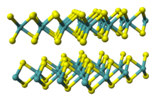
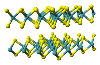
Transition-metal dichalcogenide (TMD or TMDC) monolayers are atomically thin semiconductors of the type MX2, with M a transition-metal atom (Mo, W, etc.) and X a chalcogen atom (S, Se, or Te). One layer of M atoms is sandwiched between two layers of X atoms. They are part of the large family of so-called 2D materials, named so to emphasize their extraordinary thinness. For example, a MoS2 monolayer is only 6.5 Å thick. The key feature of these materials is the interaction of large atoms in the 2D structure as compared with first-row transition-metal dichalcogenides, e.g., WTe2 exhibits anomalous giant magnetoresistance and superconductivity.

In materials science, the term single-layer materials or 2D materials refers to crystalline solids consisting of a single layer of atoms. These materials are promising for some applications but remain the focus of research. Single-layer materials derived from single elements generally carry the -ene suffix in their names, e.g. graphene. Single-layer materials that are compounds of two or more elements have -ane or -ide suffixes. 2D materials can generally be categorized as either 2D allotropes of various elements or as compounds.

A two-dimensional semiconductor is a type of natural semiconductor with thicknesses on the atomic scale. Geim and Novoselov et al. initiated the field in 2004 when they reported a new semiconducting material graphene, a flat monolayer of carbon atoms arranged in a 2D honeycomb lattice. A 2D monolayer semiconductor is significant because it exhibits stronger piezoelectric coupling than traditionally employed bulk forms. This coupling could enable applications. One research focus is on designing nanoelectronic components by the use of graphene as electrical conductor, hexagonal boron nitride as electrical insulator, and a transition metal dichalcogenide as semiconductor.

<span class="mw-page-title-main">Molybdenum ditelluride</span> Chemical compound

Molybdenum(IV) telluride, molybdenum ditelluride or just molybdenum telluride is a compound of molybdenum and tellurium with formula MoTe2, corresponding to a mass percentage of 27.32% molybdenum and 72.68% tellurium.

Platinum diselenide is a transition metal dichalcogenide with the formula PtSe2. It is a layered substance that can be split into layers down to three atoms thick. PtSe2 can behave as a metalloid or as a semiconductor depending on the thickness.

<span class="mw-page-title-main">Niobium diselenide</span> Chemical compound

Niobium diselenide or niobium(IV) selenide is a layered transition metal dichalcogenide with formula NbSe2. Niobium diselenide is a lubricant, and a superconductor at temperatures below 7.2 K that exhibit a charge density wave (CDW). NbSe2 crystallizes in several related forms, and can be mechanically exfoliated into monatomic layers, similar to other transition metal dichalcogenide monolayers. Monolayer NbSe2 exhibits very different properties from the bulk material, such as of Ising superconductivity, quantum metallic state, and strong enhancement of the CDW.

Verbeekite is a rare mineral consisting of palladium diselenide PdSe2. This transition metal dichalcogenide has an unusual monoclinic structure, with pairs of selenium atoms existing as dimers forming layers between palladium atom sheets. Unit cell dimensions are: a = 6.710, b = 4.154, c = 8.914 Å, β = 92.42 °, V = 248.24 Å3. Palladium diselenide has five polymorphs. Verbeekite can be synthesised at 11.5 GPa pressure and 1300 °C.

<span class="mw-page-title-main">Rhenium diselenide</span> Chemical compound

Rhenium diselenide is an inorganic compound with the formula ReSe2. It has a layered structure where atoms are strongly bonded within each layer. The layers are held together by weak Van der Waals bonds, and can be easily peeled off from the bulk material.

<span class="mw-page-title-main">Tantalum diselenide</span> Chemical compound

Tantalum diselenide is a compound made with tantalum and selenium atoms, with chemical formula TaSe2, which belongs to the family of transition metal dichalcogenides. In contrast to molybdenum disulfide (MoS2) or rhenium disulfide (ReS2), tantalum diselenide does not occur spontaneously in nature, but it can be synthesized. Depending on the growth parameters, different types of crystal structures can be stabilized.

References

  1. Chiu, Ming-Hui; Zhang, Chendong; Shiu, Hung-Wei; Chuu, Chih-Piao; Chen, Chang-Hsiao; Chang, Chih-Yuan S.; Chen, Chia-Hao; Chou, Mei-Yin; Shih, Chih-Kang; Li, Lain-Jong (2015). "Determination of band alignment in the single-layer MoS2/WSe2 heterojunction". Nature Communications. 6: 7666. arXiv: 1406.5137 . Bibcode:2015NatCo...6.7666C. doi:10.1038/ncomms8666. PMC   4518320 . PMID   26179885.
  2. 1 2 Agarwal, M. K.; Wani, P. A. (1979). "Growth conditions and crystal structure parameters of layer compounds in the series Mo1−xWxSe2". Materials Research Bulletin. 14 (6): 825–830. doi:10.1016/0025-5408(79)90144-2.
  3. Prakash, Abhijith; Appenzeller, Joerg (2017-02-28). "Bandgap Extraction and Device Analysis of Ionic Liquid Gated WSe2 Schottky Barrier Transistors". ACS Nano. 11 (2): 1626–1632. doi:10.1021/acsnano.6b07360. ISSN   1936-0851. PMID   28191930.
  4. Yun, Won Seok; Han, S. W.; Hong, Soon Cheol; Kim, In Gee; Lee, J. D. (2012). "Thickness and strain effects on electronic structures of transition metal dichalcogenides: 2H-MX2 semiconductors (M = Mo, W; X = S, Se, Te)". Physical Review B. 85 (3): 033305. Bibcode:2012PhRvB..85c3305Y. doi:10.1103/PhysRevB.85.033305.
  5. O'Hare, P.A.G.; Lewis, Brett M.; parkinson, B.A. (June 1988). "Standard molar enthalpy of formation by fluorine-combustion calorimetry of tungsten diselenide (WSe2). Thermodynamics of the high-temperature vaporization of WSe2. Revised value of the standard molar enthalpy of formation of molybdenite (MoS2)". The Journal of Chemical Thermodynamics. 20 (6): 681–691. doi:10.1016/0021-9614(88)90019-5.
  6. Holleman, Arnold Frederik; Wiberg, Egon (2001), Wiberg, Nils (ed.), Inorganic Chemistry, translated by Eagleson, Mary; Brewer, William, San Diego/Berlin: Academic Press/De Gruyter, ISBN   0-12-352651-5
  7. Schutte, W.J.; De Boer, J.L.; Jellinek, F. (1986). "Crystal Structures of Tungsten Disulfide and Diselenide". Journal of Solid State Chemistry. 70 (2): 207–209. Bibcode:1987JSSCh..70..207S. doi:10.1016/0022-4596(87)90057-0.
  8. 1 2 Eftekhari, Ali (2017). "Tungsten dichalcogenides (WS 2 , WSe 2 , and WTe 2 ): materials chemistry and applications". Journal of Materials Chemistry A. 5 (35): 18299–18325. doi:10.1039/C7TA04268J. ISSN   2050-7488.
  9. Ma, Yuqiang; Liu, Bilu; Zhang, Anyi; Chen, Liang; Fathi, Mohammad; Shen, Chenfei; Abbas, Ahmad N.; Ge, Mingyuan; Mecklenburg, Matthew; Zhou, Chongwu (2015-07-28). "Reversible Semiconducting-to-Metallic Phase Transition in Chemical Vapor Deposition Grown Monolayer WSe 2 and Applications for Devices". ACS Nano. 9 (7): 7383–7391. doi:10.1021/acsnano.5b02399. ISSN   1936-0851. PMID   26125321.
  10. Falin, Alexey; Holwill, Matthew; Lv, Haifeng; Gan, Wei; Cheng, Jun; Zhang, Rui; Qian, Dong; Barnett, Matthew R.; Santos, Elton J. G.; Novoselov, Konstantin S.; Tao, Tao; Wu, Xiaojun; Li, Lu Hua (23 February 2021). "Mechanical Properties of Atomically Thin Tungsten Dichalcogenides: WS 2 , WSe 2 , and WTe 2". ACS Nano. 15 (2): 2600–2610. arXiv: 2101.11869 . doi:10.1021/acsnano.0c07430. PMID   33503379. S2CID   231719536.
  11. Pouzet, J.; Bernede, J.C.; Khellil, A.; Essaidi, H.; Benhida, S. (1992). "Preparation and characterization of tungsten diselenide thin films". Thin Solid Films. 208 (2): 252–259. Bibcode:1992TSF...208..252P. doi:10.1016/0040-6090(92)90652-R.
  12. Lin, Y. C.; Björkman, T. R.; Komsa, H. P.; Teng, P. Y.; Yeh, C. H.; Huang, F. S.; Lin, K. H.; Jadczak, J.; Huang, Y. S.; Chiu, P. W.; Krasheninnikov, A. V.; Suenaga, K. (2015). "Three-fold rotational defects in two-dimensional transition metal dichalcogenides". Nature Communications. 6: 6736. Bibcode:2015NatCo...6.6736L. doi:10.1038/ncomms7736. PMC   4396367 . PMID   25832503.
  13. Mak, Kin Fai; Shan, Jie (2016). "Photonics and optoelectronics of 2D semiconductor transition metal dichalcogenides". Nature Photonics. 10 (4): 216–226. Bibcode:2016NaPho..10..216M. doi:10.1038/nphoton.2015.282. S2CID   124091327.
  14. Upadhyayula, L.C.; Loferski, J.J.; Wold, A.; Giriat, W.; Kershaw, R. (1968). "Semiconducting Properties of Single Crystals of n- and p-Type Tungsten Diselenide (WSe2)". Journal of Applied Physics. 39 (10): 353–358. Bibcode:1968JAP....39.4736U. doi:10.1063/1.1655829.
  15. Gobrecht, J.; Gerischer, H.; Tributsch, H. (1978). "Electrochemical Solar Cell Based on the d-Band Semiconductor Tungsten-Diselenide". Berichte der Bunsengesellschaft für physikalische Chemie. 82 (12): 1331–1335. doi:10.1002/bbpc.19780821212.
  16. Xia, Fengnian; Wang, Han; Xiao, Di; Dubey, Madan; Ramasubramaniam, Ashwin (2014). "Two-dimensional material nanophotonics". Nature Photonics. 8 (12): 899–907. arXiv: 1410.3882 . Bibcode:2014NaPho...8..899X. doi:10.1038/nphoton.2014.271. S2CID   14682447.
  17. Zhang, Xin; Qiao, Xiao-Fen; Shi, Wei; Wu, Jiang-Bin; Jiang, De-Sheng; Tan, Ping-Heng (2015). "Phonon and Raman scattering of two-dimensional transition metal dichalcogenides from monolayer, multilayer to bulk material". Chem. Soc. Rev. 44 (9): 2757–85. arXiv: 1502.00701 . Bibcode:2015arXiv150200701Z. doi:10.1039/C4CS00282B. PMID   25679474. S2CID   3215062.
  18. Li, Hai; Wu, Jumiati; Yin, Zongyou; Zhang, Hua (2014). "Preparation and Applications of Mechanically Exfoliated Single-Layer and Multilayer MoS2 and WSe2 Nanosheets". Accounts of Chemical Research. 47 (4): 1067–1075. doi:10.1021/ar4002312. PMID   24697842.
  19. "Tungsten diselenide shows potential for ultrathin, flexible, semi-transparent solar cells". Gizmag.com. 11 March 2014. Retrieved 17 August 2014.
  20. Florian Aigenr (10 March 2014). "Atomically thin solar cells" (Press release). Vienna University of Technology. Retrieved 18 August 2014.
  21. Lee, Sung-Joon; Lin, Zhaoyang; Huang, Jin; Choi, Christopher; Chen, Peng; Liu, Yuan; Guo, Jian; Jia, Chuancheng; Wang, Yiliu; Liao, Qingliang; Shakir, Imran; Duan, Xidong; Dunn, Bruce; Zhang, Yue; Huang, Yu; Duan, Xiangfeng (2020). "Programmable devices based on reversible solid-state doping of two-dimensional semiconductors with superionic silver iodide". Nature Electronics. 3 (10): 630–637. doi:10.1038/s41928-020-00472-x. S2CID   224896469.