Related Research Articles

Flash memory is an electronic non-volatile computer memory storage medium that can be electrically erased and reprogrammed. The two main types of flash memory, NOR flash and NAND flash, are named for the NOR and NAND logic gates. Both use the same cell design, consisting of floating gate MOSFETs. They differ at the circuit level depending on whether the state of the bit line or word lines is pulled high or low: in NAND flash, the relationship between the bit line and the word lines resembles a NAND gate; in NOR flash, it resembles a NOR gate.

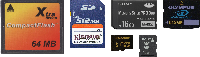
Secure Digital, officially abbreviated as SD, is a proprietary, non-volatile, flash memory card format the SD Association (SDA) developed for use in portable devices.
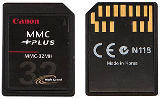
MultiMediaCard, officially abbreviated as MMC, is a memory card standard used for solid-state storage. Unveiled in 1997 by SanDisk and Siemens, MMC is based on a surface-contact low pin-count serial interface using a single memory stack substrate assembly, and is therefore much smaller than earlier systems based on high pin-count parallel interfaces using traditional surface-mount assembly such as CompactFlash. Both products were initially introduced using SanDisk NOR-based flash technology.
GDDR4 SDRAM, an abbreviation for Graphics Double Data Rate 4 Synchronous Dynamic Random-Access Memory, is a type of graphics card memory (SGRAM) specified by the JEDEC Semiconductor Memory Standard. It is a rival medium to Rambus's XDR DRAM. GDDR4 is based on DDR3 SDRAM technology and was intended to replace the DDR2-based GDDR3, but it ended up being replaced by GDDR5 within a year.
The transistor count is the number of transistors in an electronic device. It is the most common measure of integrated circuit complexity. The rate at which MOS transistor counts have increased generally follows Moore's law, which observes that transistor count doubles approximately every two years. However, being directly proportional to the area of a chip, transistor count does not represent how advanced the corresponding manufacturing technology is: a better indication of this is transistor density.

A solid-state drive (SSD) is a solid-state storage device. It provides persistent data storage using no moving parts. It is sometimes called semiconductor storage device or solid-state device; it is also called solid-state disk because it is frequently interfaced to a host system as a hard disk drive.
The Open NAND Flash Interface Working Group is a consortium of technology companies working to develop open standards for NAND flash memory and devices that communicate with them. The formation of ONFI was announced at the Intel Developer Forum in March 2006.

In electronics, a multi-level cell (MLC) is a memory cell capable of storing more than a single bit of information, compared to a single-level cell (SLC), which can store only one bit per memory cell. A memory cell typically consists of a single floating-gate MOSFET, thus multi-level cells reduce the number of MOSFETs required to store the same amount of data as single-level cells.

UniPro is a high-speed interface technology for interconnecting integrated circuits in mobile and mobile-influenced electronics. The various versions of the UniPro protocol are created within the MIPI Alliance, an organization that defines specifications targeting mobile and mobile-influenced applications.
Low-Power Double Data Rate (LPDDR), also known as LPDDR SDRAM, is a type of synchronous dynamic random-access memory that consumes less power and is targeted for mobile computers and devices such as mobile phones. Older variants are also known as Mobile DDR, and abbreviated as mDDR.
The Samsung Infuse 4G was an Android smartphone that was released by Samsung in May 2011. It has a 1.2 GHz Hummingbird processor with 8–16 GB internal Flash memory, a 4.5 inch 480×800 pixel Super AMOLED Plus capacitive touchscreen display, an 8-megapixel camera and a 1.3-megapixel front-facing camera.

The Samsung Exynos, formerly Hummingbird (Korean: 엑시노스), is a series of ARM-based system-on-chips developed by Samsung Electronics' System LSI division and manufactured by Samsung Foundry. It is a continuation of Samsung's earlier S3C, S5L and S5P line of SoCs.

HiSilicon is a Chinese fabless semiconductor company based in Shenzhen, Guangdong province and wholly owned by Huawei. HiSilicon purchases licenses for CPU designs from ARM Holdings, including the ARM Cortex-A9 MPCore, ARM Cortex-M3, ARM Cortex-A7 MPCore, ARM Cortex-A15 MPCore, ARM Cortex-A53, ARM Cortex-A57 and also for their Mali graphics cores. HiSilicon has also purchased licenses from Vivante Corporation for their GC4000 graphics core.

High Bandwidth Memory (HBM) is a computer memory interface for 3D-stacked synchronous dynamic random-access memory (SDRAM) initially from Samsung, AMD and SK Hynix. It is used in conjunction with high-performance graphics accelerators, network devices, high-performance datacenter AI ASICs, as on-package cache in CPUs and on-package RAM in upcoming CPUs, and FPGAs and in some supercomputers. The first HBM memory chip was produced by SK Hynix in 2013, and the first devices to use HBM were the AMD Fiji GPUs in 2015.
Graphics Double Data Rate 6 Synchronous Dynamic Random-Access Memory is a type of synchronous graphics random-access memory (SGRAM) with a high bandwidth, "double data rate" interface, designed for use in graphics cards, game consoles, and high-performance computing. It is a type of GDDR SDRAM, and is the successor to GDDR5. Just like GDDR5X it uses QDR in reference to the write command clock (WCK) and ODR in reference to the command clock (CK).
M-PHY is a high speed data communications physical layer protocol standard developed by the MIPI Alliance, PHY Working group, and targeted at the needs of mobile multimedia devices. The specification's details are proprietary to MIPI member organizations, but a substantial body of knowledge can be assembled from open sources. A number of industry standard settings bodies have incorporated M-PHY into their specifications including Mobile PCI Express, Universal Flash Storage, and as the physical layer for SuperSpeed InterChip USB.
The ARM Cortex-A76 is a central processing unit implementing the ARMv8.2-A 64-bit instruction set designed by ARM Holdings' Austin design centre. ARM states a 25% and 35% increase in integer and floating point performance, respectively, over a Cortex-A75 of the previous generation.
The ARM Cortex-A77 is a central processing unit implementing the ARMv8.2-A 64-bit instruction set designed by ARM Holdings' Austin design centre. ARM announced an increase of 23% and 35% in integer and floating point performance, respectively. Memory bandwidth increased 15% relative to the A76.
The ARM Cortex-A78 is a central processing unit implementing the ARMv8.2-A 64-bit instruction set designed by ARM Ltd.'s Austin centre.
The ARM Cortex-A510 is the successor to the ARM Cortex-A55 and the first ARMv9 high efficiency "LITTLE" CPU. It is the companion to the ARM Cortex-A710 "big" core. It is a clean-sheet 64-bit CPU designed by ARM Holdings' Cambridge design team.
References
- ↑ "Nokia, Others Back Mobile Memory Standard". PC World. Archived from the original on 9 February 2008.
- ↑ "JEDEC Announces Publication of Universal Flash Storage (UFS) Standard | JEDEC". www.jedec.org.
- ↑ Malykhina, Elena (14 September 2007). "Mobile Tech Companies Work On Flash Memory Standard". Information Week. Archived from the original on 12 September 2012. Retrieved 19 September 2012.
- ↑ "Toshiba Begins to Sample UFS 3.0 Drives: 96L 3D TLC NAND, Up to 2.9 GB/s". Anandtech. 23 January 2019. Retrieved 18 August 2020.
- ↑ Modine, Austin (14 September 2007). "Flash memory makers propose common card". The Channel. Retrieved 19 September 2012.
- ↑ "JEDEC Solid State Technology Association | MIPI Alliance". Archived from the original on 28 September 2011. Retrieved 15 August 2011.
- ↑ "MIPI". MIPI.
- ↑ "Universal Flash Storage (UFS) Eco-System | TOSHIBA Semiconductor & Storage Products Company | Europe(EMEA)". Archived from the original on 22 December 2015. Retrieved 26 October 2015.
- ↑ "Universal Flash Storage: Mobilize Your Data". Design Reuse. Retrieved 18 August 2020.
- ↑ "Universal Flash Storage". The Linux Kernel Archives. Retrieved 13 November 2022.
- ↑ "ufshci(4) - OpenBSD manual pages". man.openbsd.org. Retrieved 15 April 2024.
- ↑ "Evolving Mobile Solutions: Samsung at MWC 2018 | Samsung Semiconductor Global Website". www.samsung.com.
- ↑ "eUFS | Samsung Semiconductor Global Website". www.samsung.com.
- ↑ "Samsung Starts Producing First 512-Gigabyte Universal Flash Storage for Next-Generation Mobile Devices | Samsung Semiconductor Global Website". www.samsung.com.
- 1 2 "JEDEC Publishes Update to Universal Flash Storage (UFS) Standard | JEDEC". www.jedec.org. Retrieved 31 January 2020.
- ↑ Shilov, Anton. "Faster, Cheaper, Power Efficient UFS Storage: UFS 3.1 Spec Published". www.anandtech.com. Retrieved 1 February 2020.
- ↑ "Toshiba ships first NAND flash chips with faster transfer standard". PC World. 8 February 2013. Retrieved 18 August 2020.
- ↑ "The Samsung Galaxy S6 and S6 edge Review". Anandtech. 17 April 2015. Retrieved 18 August 2020.
- ↑ Shilov, Anton. "Samsung Rolls Out Its First UFS Cards: SSD Performance in Card Form-Factor" . Retrieved 7 July 2016.
- ↑ "Qualcomm Snapdragon 865 to sport LPDDR5X RAM, UFS 3.0, will come in 2 variants: Report". First Post. 18 June 2019. Retrieved 18 August 2020.
- ↑ "OnePlus 7 Pro confirmed to feature UFS 3.0 flash storage". Android Central. 6 May 2019. Retrieved 18 August 2020.
- ↑ Universal Flash Storage Association (3 January 2020). "UFSA Widens UFS Ecosystem, Adding Vendors of Removable Mobile Cards and Related Technology". Business Wire. Austin, Texas. Retrieved 22 November 2020.
"UFS Cards will play a critical role[...]" said Hangu Sohn, vice president of NAND Memory Planning at Samsung Electronics. "Moreover, with a royalty-free form factor and open standard design, we expect to see a rapid transition to these cards in 2020."
- ↑ "UFS 4.0 Specifications, Speed Test, UFS 4.0 vs UFS 3.1". 6 July 2023. Retrieved 28 February 2024.
- ↑ "JEDEC Announces Publication of Universal Flash Storage (UFS) Standard | JEDEC". www.jedec.org. Retrieved 8 May 2017.
- ↑ "JEDEC Updates Universal Flash Storage (UFS) Standard | JEDEC". www.jedec.org. Retrieved 8 May 2017.
- ↑ "JEDEC Publishes Universal Flash Storage (UFS) Standard v2.0 | JEDEC". www.jedec.org. Retrieved 8 May 2017.
- ↑ "JEDEC Updates Universal Flash Storage (UFS) and Related Standards | JEDEC". www.jedec.org. Retrieved 8 May 2017.
- ↑ "UNIVERSAL FLASH STORAGE, UFS 2.2". www.jedec.org. Retrieved 31 July 2021.
- 1 2 "JEDEC Publishes Universal Flash Storage (UFS & UFSHCI) Version 3.0 and UFS Card Extension Version 1.1". www.jedec.org. Retrieved 31 January 2018.
- ↑ "JEDEC Updates Universal Flash Storage (UFS) and Supporting Memory Interface Standard". www.jedec.org. Retrieved 18 September 2022.
- ↑ "JEDEC Publishes Universal Flash Storage (UFS) Removable Card Standard | JEDEC". www.jedec.org. Retrieved 30 October 2017.
- ↑ "JEDEC Advances Universal Flash Storage (UFS) Removable Card Standard 3.0". www.jedec.org. Retrieved 31 July 2021.
- ↑ "Exynos 9609 Mobile Processor: Specs, Features | Samsung Exynos". Samsung Semiconductor. Retrieved 26 January 2020.
- ↑ "Exynos 9610 Processor: Specs, Features | Samsung Exynos". Samsung Semiconductor. Retrieved 26 January 2020.
- ↑ "Exynos 9611 Mobile Processor: Specs, Features | Samsung Exynos". Samsung Semiconductor. Retrieved 26 January 2020.
- ↑ "Exynos 980 5G Mobile Processor: Specs, Features | Samsung Exynos". Samsung Semiconductor. Retrieved 26 January 2020.
- ↑ "Exynos 9 Series 9820 Processor: Specs, Features | Samsung Exynos". Samsung Semiconductor. Retrieved 14 November 2018.
- ↑ Cutress, Ian (6 September 2019). "Huawei Announces Kirin 990 and Kirin 990 5G: Dual SoC Approach, Integrated 5G Modem". AnandTech. Archived from the original on 6 September 2019.
- ↑ "Qualcomm Snapdragon 888: specs and benchmarks". NanoReview.net. Retrieved 22 February 2021.
- ↑ "Exynos 2100 5G Mobile Processor: Specs, Features". Samsung.com. Retrieved 27 June 2021.
- ↑ "Exynos 2200 | Processor | Samsung Semiconductor". www.samsung.com.
- ↑ "Snapdragon-8-Gen-2-Product-Brief.pdf" (PDF). Qualcomm. Retrieved 19 November 2022.
- ↑ "JEDEC Publishes Universal Flash Storage (UFS) Removable Card Standard | JEDEC". www.jedec.org. Retrieved 7 July 2016.
- ↑ "Standards & Documents Search | JEDEC". www.jedec.org.
- ↑ "Standards & Documents Search | JEDEC". www.jedec.org.
- ↑ "Standards & Documents Search | JEDEC". www.jedec.org.
- ↑ "UNIVERSAL FLASH STORAGE (UFS) CARD EXTENSION, Version 3.0 | JEDEC". www.jedec.org.
- ↑ "UFS (Universal Flash Storage) | JEDEC". www.jedec.org.
- ↑ "SSD Lifespan: How Long Will Your SSD Work?". Enterprise Storage Forum. 1 March 2019. Retrieved 18 August 2020.