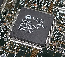
VLSI Technology, Inc., was an American company that designed and manufactured custom and semi-custom integrated circuits (ICs). The company was based in Silicon Valley, with headquarters at 1109 McKay Drive in San Jose. Along with LSI Logic, VLSI Technology defined the leading edge of the application-specific integrated circuit (ASIC) business, which accelerated the push of powerful embedded systems into affordable products.
Initially the company often referred to itself as "VTI" (for VLSI Technology Inc.), and adopted a distinctive "VTI" logo. But it was forced to drop that designation in the mid-1980s because of a trademark conflict.
The company was founded in 1979, by a trio from Fairchild Semiconductor by way of Synertek – Jack Balletto, Dan Floyd, and Gunnar Wetlesen – and by Doug Fairbairn of Xerox PARC and Lambda (later VLSI Design) magazine.
Alfred J. Stein became the CEO of the company in 1982. Subsequently, VLSI built its first fab in San Jose; eventually a second fab was built in San Antonio, Texas. VLSI had its initial public offering on February 23, 1983, in which 4,000,000 shares were sold at $13 a share.[1] It was listed on the stock market as (Nasdaq:VLSI). The company was acquired in 1999 by Philips for $21 a share,[2] and survives to this day as part of NXP Semiconductors.
The original business plan was to be a contract wafer fabrication company, but the venture investors wanted the company to develop IC (Integrated Circuit) design tools to help fill the foundry.
Thanks to its Caltech and UC Berkeley students, VLSI was an important pioneer in the electronic design automation (EDA) industry. It offered a sophisticated package of tools, originally based on the 'lambda-based' design style advocated by Carver Mead and Lynn Conway.[3]
An early challenge for the fledgling company was the so-called Bagpipe project. In January 1982, Steve Jobs approached a group of VLSI Technology managers including Jack Balletto with a request: Would they help Apple Inc. build a custom chip for the not-yet-announced Macintosh computer? In spite of the fact that VLSI's design tools were still in their infancy, the offer proved irresistible because of the prestige the chip would confer on the company if successful. For the VLSI Technology engineering team, this project became an all-hands-on-deck effort. Working side by side with Apple engineers Burrell Smith and Martin Haeberli, the group delivered a packaged prototype by September. Although the chip (referred to as the Integrated Burrell Machine) was functional, its performance fell short of expectations, and schedule pressures caused Apple to drop the chip in favor of a more conservative design – a big disappointment for VLSI Technology.[4][5]
VLSI became an early vendor of standard cell (cell-based technology) to the merchant market in the early 1980s where the other ASIC-focused company, LSI Logic, was a leader in gate arrays. Prior to VLSI's cell-based offering, the technology had been primarily available only within large vertically integrated companies with semiconductor units such as AT&T and IBM.
VLSI's design tools included not only design entry and simulation but eventually also cell-based routing (chip compiler), a datapath compiler, SRAM and ROM compilers, and a state machine compiler. The tools were an integrated design solution for IC design and not just point tools, or more general purpose system tools. A designer could edit transistor-level polygons and/or logic schematics, then run DRC and LVS, extract parasitics from the layout and run Spice simulation, then back-annotate the timing or gate size changes into the logic schematic database. Characterization tools were integrated to generate FrameMaker Data Sheets for Libraries.
In March 1991, VLSI spun off its IC design tools group into a wholly owned subsidiary, Compass Design Automation.[6] The Compass subsidiary was purchased by Avanti Corporation in 1997.
VLSI's physical design tools were critical not only to its ASIC business, but also acted as significant drivers for the broader electronic design automation (EDA) industry. When VLSI and its main ASIC competitor, LSI Logic, were establishing the ASIC industry, commercially available tools could not deliver the productivity necessary to support the physical design of hundreds of ASIC designs each year without the deployment of a substantial number of layout engineers. The companies' development of automated layout tools was driven by a judgement that other in-market products were not sufficient or adaptable enough for VLSI's use case. Other significant market entrants with similar capabilities arrived in late 1980s when Tangent Systems released its TanCell and TanGate products. In 1989, Tangent was acquired by Cadence Design Systems (founded in 1988).
By the early 1990s, VLSI had not been timely in adopting a 1.0μm manufacturing process as the rest of the industry moved to that geometry in the late 1980s. VLSI entered a long-term technology partnership with Hitachi and finally released a 1.0μm process and cell library (actually more of a 1.2μm library with a 1.0μm gate).
As VLSI struggled to gain parity with the rest of the industry in semiconductor technology, the design flow was moving rapidly to a Verilog HDL and synthesis flow. Cadence acquired Gateway, the leader in Verilog hardware design language (HDL) and Synopsys was dominating the exploding field of design synthesis. As VLSI's tools were being eclipsed, VLSI waited too long to open the tools up to other fabs and Compass Design Automation was never a viable competitor to industry leaders.
Meanwhile, VLSI entered the merchant high speed static RAM (SRAM) market as they needed a product to drive the semiconductor process technology development. All the large semiconductor companies built high speed SRAMs with cost structures VLSI could never match. VLSI withdrew once it was clear that the Hitachi process technology partnership was working.
ARM Ltd was formed in 1990 as a semiconductor intellectual property licensor, backed by Acorn, Apple, and VLSI. VLSI became a licensee of the powerful ARM processor. Initial adoption of the ARM processor was slow. Few applications could justify the overhead of an embedded 32-bit processor. In fact, despite the addition of further licensees, the ARM processor enjoyed little market success until they developed the novel 'Thumb' extensions. Ericsson adopted the ARM processor in a VLSI chipset for its GSM handset designs in the early 1990s. It was the GSM boost that is the foundation of ARM the company/technology that it is today.
In the early 1990s, VLSI produced a first-party PC chipset. This product was developed by five engineers using the "Megacells" in the VLSI library. In time, this business developed into a significant revenue stream. The chipsets designed and manufactured by VLSI integrated much of the peripheral I/O logic and thereby substantially lowered the cost of PCs that used Intel or Motorola processors. This included the early Apple Power Macintosh PCs which used the Motorola 68030 and 68040. Some innovations included the integration of PCI bridge logic and the GraphiCore 2D graphics accelerator.
The GraphiCore project was formed and led by Desi Rhoden in 1994. It was notable for being a fresh design, without the baggage of legacy EGA/VGA logic, and for direct support of synchronous DRAM, the forerunner of DDR memory. Desi Rhoden later founded AMI, a consortium of all the major DRAM vendors, which created important standards in DDR memory design. VLSI eventually ceded the chipset market to Intel because Intel was able to package-sell its processors, chipsets, and even board-level products together.
VLSI also had an early partnership with PMC, a design group that had been nurtured of British Columbia Bell. When PMC wanted to divest its semiconductor intellectual property venture, VLSI's bid was beaten by a creative deal by Sierra Semiconductor. The telecom business unit management at VLSI opted to go it alone. PMC Sierra became one of the most important telecom ASSP vendors.
Scientists and innovations from the 'design technology' part of VLSI found their way to Cadence Design Systems (by way of Redwood Design Automation). Compass Design Automation (VLSI's CAD and Library spin-off) was sold to Avant! Corporation, which itself was acquired by Synopsys.
Global expansion, ARM, GSM and Philips/NXP
VLSI maintained operations throughout the US, and in Britain, France, Germany, Italy, Japan, Singapore and Taiwan. One of its key sites was in Tempe, Arizona, where a family of highly successful chipsets was developed for IBM PC compatible motherboards and early Apple Power Macintosh PCs.
VLSI's design office in Richardson, Texas, was responsible for the design of many large, standard cell ASICS in the 1990s, including the first floating-point co-processors for Cyrix and Digital signal processors for telecom switching and echo-cancellation equipment for Alcatel-Lucent.
In 1990, VLSI Technology, Acorn Computers, and Apple Computer were the founding investing partners in ARM Ltd. VLSI Technology was the only manufacturer of chips using ARM cores at that time, as well as the only designer of ASICs using ARM.
In 1997, VLSI Technology offered the first ARM chipset for Set-top box vendors for the cable and satellite TV industries named VISTA (VLSI Integrated Set-Top Architecture). Previously, STB chipsets were custom designed for single customers only and were not available to the emerging merchant market. But, VISTA was a merchant market, 4-chip set that featured an ARM7TDMI processor core, transport and demux and a Mediamatics MPEG 1/2 decoder with On Screen Display logic.
Ericsson of Sweden, after many years of collaboration, was by 1998 VLSI's largest customer, with annual revenue of $120 million. VLSI's datapath compiler (VDP) was the value-added differentiator that opened the door at Ericsson in 1987–1988. The silicon revenue and GPM enabled by VDP must make it one of the most successful pieces of customer-configurable, non-memory silicon intellectual property (SIP) in the history of the industry. Within the Wireless Products division, based at Sophia-Antipolis in France, VLSI developed a range of algorithms and circuits for the GSM standard and for cordless standards such as the European DECT and the Japanese PHS.
Stimulated by its growth and success in the wireless handset IC area, Philips Electronics acquired VLSI in June 1999, for about $1 billion. The former components survive to this day as part of Philips spin-off NXP Semiconductors.
Products
This section needs expansion. You can help by adding to it. (November 2014)
A field-programmable gate array (FPGA) is a type of configurable integrated circuit that can be repeatedly programmed post manufacturing. FPGAs are a subset of logic devices referred to as programmable logic devices ("PLDs"). They consist of an array of programmable logic blocks with a connecting grid, that can be configured "in the field" to interconnect with other logic blocks to perform various digital functions. FPGAs are often used in limited (low) quantity production of custom-made products, and in research and development, where the higher cost of individual FPGAs is not as important, and where creating and manufacturing a custom circuit wouldn't be feasible. Other applications for FPGAs include the telecommunications, automotive, aerospace, and industrial sectors, which benefit from their flexibility, high signal processing speed, and parallel processing abilities.
An integrated circuit (IC), also known as a microchip, computer chip, or simply chip, is a small electronic device made up of multiple interconnected electronic components such as transistors, resistors, and capacitors. These components are etched onto a small piece of semiconductor material, usually silicon. Integrated circuits are used in a wide range of electronic devices, including computers, smartphones, and televisions, to perform various functions such as processing and storing information. They have greatly impacted the field of electronics by enabling device miniaturization and enhanced functionality.
Very-large-scale integration (VLSI) is the process of creating an integrated circuit (IC) by combining millions or billions of MOS transistors onto a single chip. VLSI began in the 1970s when MOS integrated circuit chips were developed and then widely adopted, enabling complex semiconductor and telecommunication technologies. The microprocessor and memory chips are VLSI devices.
Complementary metal–oxide–semiconductor is a type of metal–oxide–semiconductor field-effect transistor (MOSFET) fabrication process that uses complementary and symmetrical pairs of p-type and n-type MOSFETs for logic functions. CMOS technology is used for constructing integrated circuit (IC) chips, including microprocessors, microcontrollers, memory chips, and other digital logic circuits. CMOS technology is also used for analog circuits such as image sensors, data converters, RF circuits, and highly integrated transceivers for many types of communication.
An application-specific integrated circuit is an integrated circuit (IC) chip customized for a particular use, rather than intended for general-purpose use, such as a chip designed to run in a digital voice recorder or a high-efficiency video codec. Application-specific standard product chips are intermediate between ASICs and industry standard integrated circuits like the 7400 series or the 4000 series. ASIC chips are typically fabricated using metal–oxide–semiconductor (MOS) technology, as MOS integrated circuit chips.
Electronic design automation (EDA), also referred to as electronic computer-aided design (ECAD), is a category of software tools for designing electronic systems such as integrated circuits and printed circuit boards. The tools work together in a design flow that chip designers use to design and analyze entire semiconductor chips. Since a modern semiconductor chip can have billions of components, EDA tools are essential for their design; this article in particular describes EDA specifically with respect to integrated circuits (ICs).
In a computer system, a chipset is a set of electronic components on one or more integrated circuits that manages the data flow between the processor, memory and peripherals. The chipset is usually found on the motherboard of computers. Chipsets are usually designed to work with a specific family of microprocessors. Because it controls communications between the processor and external devices, the chipset plays a crucial role in determining system performance.
A gate array is an approach to the design and manufacture of application-specific integrated circuits (ASICs) using a prefabricated chip with components that are later interconnected into logic devices according to custom order by adding metal interconnect layers in the factory. It was popular during the upheaval in the semiconductor industry in the 1980s, and its usage declined by the end of the 1990s.
Fabless manufacturing is the design and sale of hardware devices and semiconductor chips while outsourcing their fabrication to a specialized manufacturer called a semiconductor foundry. These foundries are typically, but not exclusively, located in the United States, China, and Taiwan. Fabless companies can benefit from lower capital costs while concentrating their research and development resources on the end market. Some fabless companies and pure play foundries may offer integrated-circuit design services to third parties.
Nordic Semiconductor ASA was founded in 1983 and is a Norwegian fabless technology company with its headquarters in Trondheim, Norway. The company specializes in designing ultra-low-power wireless communication semiconductors and supporting software for engineers developing and manufacturing Internet of Things (IoT) products.
A mixed-signal integrated circuit is any integrated circuit that has both analog circuits and digital circuits on a single semiconductor die. Their usage has grown dramatically with the increased use of cell phones, telecommunications, portable electronics, and automobiles with electronics and digital sensors.
Cirrus Logic Inc. is an American fabless semiconductor supplier that specializes in analog, mixed-signal, and audio DSP integrated circuits (ICs). Since 1998, the company's headquarters have been in Austin, Texas.
In semiconductor design, standard-cell methodology is a method of designing application-specific integrated circuits (ASICs) with mostly digital-logic features. Standard-cell methodology is an example of design abstraction, whereby a low-level very-large-scale integration (VLSI) layout is encapsulated into an abstract logic representation.
Integrated circuit design, semiconductor design, chip design or IC design, is a sub-field of electronics engineering, encompassing the particular logic and circuit design techniques required to design integrated circuits, or ICs. ICs consist of miniaturized electronic components built into an electrical network on a monolithic semiconductor substrate by photolithography.
The R4000 is a microprocessor developed by MIPS Computer Systems that implements the MIPS III instruction set architecture (ISA). Officially announced on 1 October 1991, it was one of the first 64-bit microprocessors and the first MIPS III implementation. In the early 1990s, when RISC microprocessors were expected to replace CISC microprocessors such as the Intel i486, the R4000 was selected to be the microprocessor of the Advanced Computing Environment (ACE), an industry standard that intended to define a common RISC platform. ACE ultimately failed for a number of reasons, but the R4000 found success in the workstation and server markets.
The transistor count is the number of transistors in an electronic device. It is the most common measure of integrated circuit complexity. The rate at which MOS transistor counts have increased generally follows Moore's law, which observes that transistor count doubles approximately every two years. However, being directly proportional to the area of a die, transistor count does not represent how advanced the corresponding manufacturing technology is. A better indication of this is transistor density which is the ratio of a semiconductor's transistor count to its die area.
The IEEE Robert N. Noyce Medal is a science award presented by the IEEE for outstanding contributions to the microelectronics industry. It is given to individuals who have demonstrated contributions in multiple areas including technology development, business development, industry leadership, development of technology policy, and standards development. The medal is named in honour of Robert N. Noyce, the co-founder of Intel Corporation. He was also renowned for his 1959 invention of the integrated circuit. The medal is funded by Intel Corporation and was first awarded in 2000.
The R2000 is a 32-bit microprocessor chip set developed by MIPS Computer Systems that implemented the MIPS I instruction set architecture (ISA). Introduced in January 1986, it was the first commercial implementation of the MIPS architecture and the first commercial RISC processor available to all companies. The R2000 competed with Digital Equipment Corporation (DEC) VAX minicomputers and with Motorola 68000 and Intel Corporation 80386 microprocessors. R2000 users included Ardent Computer, DEC, Silicon Graphics, Northern Telecom and MIPS's own Unix workstations.
LSI Logic Corporation, was an American company founded in Santa Clara, California, was a pioneer in the ASIC and EDA industries. It evolved over time to design and sell semiconductors and software that accelerated storage and networking in data centers, mobile networks and client computing.
↑ Andy Herzfeld. Revolution in the Valley: The Insanely Great Story of How the Mac Was Made. O'Reilly 2005. p. 122, where the company is erroneously identified as VLSI Design.
↑ Computer History Museum. Interview with Douglas Fairbairn. 6 October 2016. Oral History Collection catalog number 102717219. Accessed 11 November 2019.
This page is based on this Wikipedia article Text is available under the CC BY-SA 4.0 license; additional terms may apply. Images, videos and audio are available under their respective licenses.