Related Research Articles
A charge-coupled device (CCD) is an integrated circuit containing an array of linked, or coupled, capacitors. Under the control of an external circuit, each capacitor can transfer its electric charge to a neighboring capacitor. CCD sensors are a major technology used in digital imaging.
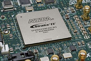
A field-programmable gate array (FPGA) is an integrated circuit designed to be configured by a customer or a designer after manufacturing – hence the term "field-programmable". The FPGA configuration is generally specified using a hardware description language (HDL), similar to that used for an application-specific integrated circuit (ASIC). Circuit diagrams were previously used to specify the configuration, but this is increasingly rare due to the advent of electronic design automation tools.

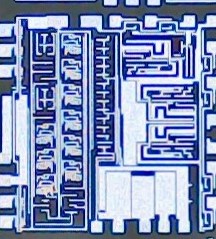
An integrated circuit or monolithic integrated circuit is a set of electronic circuits on one small flat piece of semiconductor material that is normally silicon. The integration of large numbers of tiny MOS transistors into a small chip results in circuits that are orders of magnitude smaller, faster, and less expensive than those constructed of discrete electronic components. The IC's mass production capability, reliability, and building-block approach to integrated circuit design has ensured the rapid adoption of standardized ICs in place of designs using discrete transistors. ICs are now used in virtually all electronic equipment and have revolutionized the world of electronics. Computers, mobile phones, and other digital home appliances are now inextricable parts of the structure of modern societies, made possible by the small size and low cost of ICs.
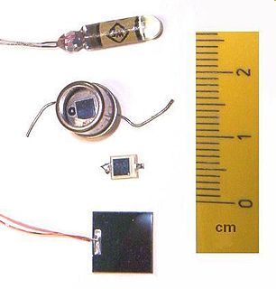
A photodiode is a semiconductor p-n junction device that converts light into an electrical current. The current is generated when photons are absorbed in the photodiode. Photodiodes may contain optical filters, built-in lenses, and may have large or small surface areas. Photodiodes usually have a slower response time as their surface area increases. The common, traditional solar cell used to generate electric solar power is a large area photodiode.
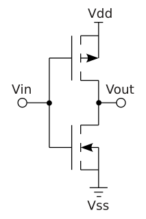
Complementary metal–oxide–semiconductor (CMOS), also known as complementary-symmetry metal–oxide–semiconductor (COS-MOS), is a type of metal–oxide–semiconductor field-effect transistor (MOSFET) fabrication process that uses complementary and symmetrical pairs of p-type and n-type MOSFETs for logic functions. CMOS technology is used for constructing integrated circuit (IC) chips, including microprocessors, microcontrollers, memory chips, and other digital logic circuits. CMOS technology is also used for analog circuits such as image sensors, data converters, RF circuits, and highly integrated transceivers for many types of communication.

The transputer is a series of pioneering microprocessors from the 1980s, featuring integrated memory and serial communication links, intended for parallel computing. They were designed and produced by Inmos, a semiconductor company based in Bristol, United Kingdom.
Digital image processing is the use of a digital computer to process digital images through an algorithm. As a subcategory or field of digital signal processing, digital image processing has many advantages over analog image processing. It allows a much wider range of algorithms to be applied to the input data and can avoid problems such as the build-up of noise and distortion during processing. Since images are defined over two dimensions digital image processing may be modeled in the form of multidimensional systems. The generation and development of digital image processing are mainly affected by three factors: first, the development of computers; second, the development of mathematics ; third, the demand for a wide range of applications in environment, agriculture, military, industry and medical science has increased.
In electronics and especially synchronous digital circuits, a clock signal oscillates between a high and a low state and is used like a metronome to coordinate actions of digital circuits.

A Bayer filter mosaic is a color filter array (CFA) for arranging RGB color filters on a square grid of photosensors. Its particular arrangement of color filters is used in most single-chip digital image sensors used in digital cameras, camcorders, and scanners to create a color image. The filter pattern is 50% green, 25% red and 25% blue, hence is also called BGGR,RGBG, GRBG, or RGGB.
The R420 GPU, developed by ATI Technologies, was the company's basis for its 3rd-generation DirectX 9.0/OpenGL 2.0-capable graphics cards. Used first on the Radeon X800, the R420 was produced on a 0.13 micrometer low-K photolithography process and used GDDR-3 memory. The chip was designed for AGP graphics cards.
A mixed-signal integrated circuit is any integrated circuit that has both analog circuits and digital circuits on a single semiconductor die.
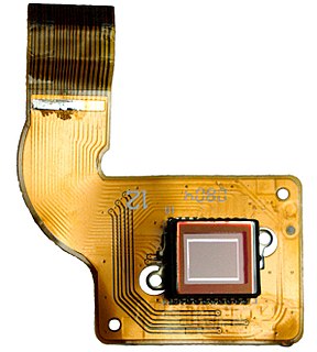
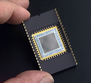
An image sensor or imager is a sensor that detects and conveys information used to make an image. It does so by converting the variable attenuation of light waves into signals, small bursts of current that convey the information. The waves can be light or other electromagnetic radiation. Image sensors are used in electronic imaging devices of both analog and digital types, which include digital cameras, camera modules, camera phones, optical mouse devices, medical imaging equipment, night vision equipment such as thermal imaging devices, radar, sonar, and others. As technology changes, electronic and digital imaging tends to replace chemical and analog imaging.

An active-pixel sensor (APS) is an image sensor where each pixel sensor unit cell has a photodetector and one or more active transistors. In a metal–oxide–semiconductor (MOS) active-pixel sensor, MOS field-effect transistors (MOSFETs) are used as amplifiers. There are different types of APS, including the early NMOS APS and the much more common complementary MOS (CMOS) APS, also known as the CMOS sensor, which is widely used in digital camera technologies such as cell phone cameras, web cameras, most modern digital pocket cameras, most digital single-lens reflex cameras (DSLRs), and mirrorless interchangeable-lens cameras (MILCs). CMOS sensors emerged as an alternative to charge-coupled device (CCD) image sensors and eventually outsold them by the mid-2000s.
OmniVision Technologies Inc. is a Chinese company that is publicly traded as part of Will Semiconductor. The company designs and develops digital imaging products for use in mobile phones, notebooks, netbooks and webcams, security and surveillance cameras, entertainment, automotive and medical imaging systems. Headquartered in Santa Clara, California, OmniVision Technologies has offices in the US, Western Europe and Asia.

Medipix is a family of photon counting and particle tracking pixel detectors developed by an international collaboration, hosted by CERN.

In electronic engineering, a through-silicon via (TSV) or through-chip via is a vertical electrical connection (via) that passes completely through a silicon wafer or die. TSVs are high-performance interconnect techniques used as an alternative to wire-bond and flip chips to create 3D packages and 3D integrated circuits. Compared to alternatives such as package-on-package, the interconnect and device density is substantially higher, and the length of the connections becomes shorter.
A massively parallel processor array, also known as a multi purpose processor array (MPPA) is a type of integrated circuit which has a massively parallel array of hundreds or thousands of CPUs and RAM memories. These processors pass work to one another through a reconfigurable interconnect of channels. By harnessing a large number of processors working in parallel, an MPPA chip can accomplish more demanding tasks than conventional chips. MPPAs are based on a software parallel programming model for developing high-performance embedded system applications.

A back-illuminated sensor, also known as backside illumination sensor, is a type of digital image sensor that uses a novel arrangement of the imaging elements to increase the amount of light captured and thereby improve low-light performance.
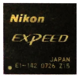
The Nikon Expeed image/video processors are media processors for Nikon's digital cameras. They perform a large number of tasks: Bayer filtering, demosaicing, image sensor corrections/dark-frame subtraction, image noise reduction, image sharpening, image scaling, gamma correction, image enhancement/Active D-Lighting, colorspace conversion, chroma subsampling, framerate conversion, lens distortion/chromatic aberration correction, image compression/JPEG encoding, video compression, display/video interface driving, digital image editing, face detection, audio processing/compression/encoding and computer data storage/data transmission.
An oversampled binary image sensor is an image sensor with non-linear response capabilities reminiscent of traditional photographic film. Each pixel in the sensor has a binary response, giving only a one-bit quantized measurement of the local light intensity. The response function of the image sensor is non-linear and similar to a logarithmic function, which makes the sensor suitable for high dynamic range imaging.
References
- "Xetal: a low-power high-performance smart camera processor" by Kleihorst et al. Published in The 2001 IEEE International Symposium on Circuits and Systems, Volume 5