Image sensor

Last updated
A CCD image sensor on a flexible circuit board Ccd-sensor.jpg
A CCD image sensor on a flexible circuit board
An American Microsystems, Inc., (AMI) 1-kilobit DRAM chip (center chip with glass window) used as an image sensor by the Cromemco Cyclops Cromemco Cyclops Camera Board 1.jpg
An American Microsystems, Inc., (AMI) 1-kilobit DRAM chip (center chip with glass window) used as an image sensor by the Cromemco Cyclops

An image sensor or imager is a sensor that detects and conveys information used to form an image. It does so by converting the variable attenuation of light waves (as they pass through or reflect off objects) into signals, small bursts of current that convey the information. The waves can be light or other electromagnetic radiation. Image sensors are used in electronic imaging devices of both analog and digital types, which include digital cameras, camera modules, camera phones, optical mouse devices, [1] [2] [3] medical imaging equipment, night vision equipment such as thermal imaging devices, radar, sonar, and others. As technology changes, electronic and digital imaging tends to replace chemical and analog imaging.

Contents

The two main types of electronic image sensors are the charge-coupled device (CCD) and the active-pixel sensor (CMOS sensor). Both CCD and CMOS sensors are based on metal–oxide–semiconductor (MOS) technology, with CCDs based on MOS capacitors and CMOS sensors based on MOSFET (MOS field-effect transistor) amplifiers. Analog sensors for invisible radiation tend to involve vacuum tubes of various kinds, while digital sensors include flat-panel detectors.

CCD vs. CMOS sensors

A micrograph of the corner of the photosensor array of a webcam digital camera A micrograph of the corner of the photosensor array of a 'webcam'.jpeg
A micrograph of the corner of the photosensor array of a webcam digital camera
Image sensor (upper left) on the motherboard of a Nikon Coolpix L2 6 MP Image sensor and motherbord nikon coolpix l2.JPG
Image sensor (upper left) on the motherboard of a Nikon Coolpix L2 6 MP

The two main types of digital image sensors are the charge-coupled device (CCD) and the active-pixel sensor (CMOS sensor), fabricated in complementary MOS (CMOS) or N-type MOS (NMOS or Live MOS) technologies. Both CCD and CMOS sensors are based on the MOS technology, [4] with MOS capacitors being the building blocks of a CCD, [5] and MOSFET amplifiers being the building blocks of a CMOS sensor. [6] [7]

Cameras integrated in small consumer products generally use CMOS sensors, which are usually cheaper and have lower power consumption in battery powered devices than CCDs. [8] CCD sensors are used for high end broadcast quality video cameras, and CMOS sensors dominate in still photography and consumer goods where overall cost is a major concern. Both types of sensor accomplish the same task of capturing light and converting it into electrical signals.

Each cell of a CCD image sensor is an analog device. When light strikes the chip it is held as a small electrical charge in each photo sensor. The charges in the line of pixels nearest to the (one or more) output amplifiers are amplified and output, then each line of pixels shifts its charges one line closer to the amplifiers, filling the empty line closest to the amplifiers. This process is then repeated until all the lines of pixels have had their charge amplified and output. [9]

A CMOS image sensor has an amplifier for each pixel compared to the few amplifiers of a CCD. This results in less area for the capture of photons than a CCD, but this problem has been overcome by using microlenses in front of each photodiode, which focus light into the photodiode that would have otherwise hit the amplifier and not been detected. [9] Some CMOS imaging sensors also use Back-side illumination to increase the number of photons that hit the photodiode. [10] CMOS sensors can potentially be implemented with fewer components, use less power, and/or provide faster readout than CCD sensors. [11] They are also less vulnerable to static electricity discharges.

Another design, a hybrid CCD/CMOS architecture (sold under the name "sCMOS") consists of CMOS readout integrated circuits (ROICs) that are bump bonded to a CCD imaging substrate – a technology that was developed for infrared staring arrays and has been adapted to silicon-based detector technology. [12] Another approach is to utilize the very fine dimensions available in modern CMOS technology to implement a CCD like structure entirely in CMOS technology: such structures can be achieved by separating individual poly-silicon gates by a very small gap; though still a product of research hybrid sensors can potentially harness the benefits of both CCD and CMOS imagers. [13]

Performance

There are many parameters that can be used to evaluate the performance of an image sensor, including dynamic range, signal-to-noise ratio, and low-light sensitivity. For sensors of comparable types, the signal-to-noise ratio and dynamic range improve as the size increases. It is because in a given integration (exposure) time, more photons hit the pixel with larger area.

Exposure-time control

Exposure time of image sensors is generally controlled by either a conventional mechanical shutter, as in film cameras, or by an electronic shutter. Electronic shuttering can be "global," in which case the entire image sensor area's accumulation of photoelectrons starts and stops simultaneously, or "rolling" in which case the exposure interval of each row immediate precedes that row's readout, in a process that "rolls" across the image frame (typically from top to bottom in landscape format). Global electronic shuttering is less common, as it requires "storage" circuits to hold charge from the end of the exposure interval until the readout process gets there, typically a few milliseconds later. [14]

Color separation

Bayer pattern on sensor Bayer pattern on sensor profile.svg
Bayer pattern on sensor
Foveon's scheme of vertical filtering for color sensing Absorption-X3.svg
Foveon's scheme of vertical filtering for color sensing

There are several main types of color image sensors, differing by the type of color-separation mechanism:

Specialty sensors

Infrared view of the Orion Nebula taken by ESO's HAWK-I, a cryogenic wide-field imager A deep infrared view of the Orion Nebula from HAWK-I - Eso1625a.jpg
Infrared view of the Orion Nebula taken by ESO's HAWK-I, a cryogenic wide-field imager

Special sensors are used in various applications such as thermography, creation of multi-spectral images, video laryngoscopes, gamma cameras, sensor arrays for x-rays, and other highly sensitive arrays for astronomy. [20]

While in general, digital cameras use a flat sensor, Sony prototyped a curved sensor in 2014 to reduce/eliminate Petzval field curvature that occurs with a flat sensor. Use of a curved sensor allows a shorter and smaller diameter of the lens with reduced elements and components with greater aperture and reduced light fall-off at the edge of the photo. [21]

History

Early analog sensors for visible light were video camera tubes. They date back to the 1930s, and several types were developed up until the 1980s. By the early 1990s, they had been replaced by modern solid-state CCD image sensors. [22]

The basis for modern solid-state image sensors is MOS technology, [23] [24] which originates from the invention of the MOSFET by Mohamed M. Atalla and Dawon Kahng at Bell Labs in 1959. [25] Later research on MOS technology led to the development of solid-state semiconductor image sensors, including the charge-coupled device (CCD) and later the active-pixel sensor (CMOS sensor). [23] [24]

The passive-pixel sensor (PPS) was the precursor to the active-pixel sensor (APS). [7] A PPS consists of passive pixels which are read out without amplification, with each pixel consisting of a photodiode and a MOSFET switch. [26] It is a type of photodiode array, with pixels containing a p-n junction, integrated capacitor, and MOSFETs as selection transistors. A photodiode array was proposed by G. Weckler in 1968. [6] This was the basis for the PPS. [7] These early photodiode arrays were complex and impractical, requiring selection transistors to be fabricated within each pixel, along with on-chip multiplexer circuits. The noise of photodiode arrays was also a limitation to performance, as the photodiode readout bus capacitance resulted in increased noise level. Correlated double sampling (CDS) could also not be used with a photodiode array without external memory. [6] However, in 1914 Deputy Consul General Carl R. Loop, reported to the state department in a Consular Report on Archibald M. Low's Televista system that "It is stated that the selenium in the transmitting screen may be replaced by any diamagnetic material". [27]

In June 2022, Samsung Electronics announced that it had created a 200 million pixel image sensor. The 200MP ISOCELL HP3 has 0.56 micrometer pixels with Samsung reporting that previous sensors had 0.64 micrometer pixels, a 12% decrease since 2019. The new sensor contains 200 million pixels in a 1-by-1.4-inch (25 by 36 mm) lens. [28]

Charge-coupled device

The charge-coupled device (CCD) was invented by Willard S. Boyle and George E. Smith at Bell Labs in 1969. [29] While researching MOS technology, they realized that an electric charge was the analogy of the magnetic bubble and that it could be stored on a tiny MOS capacitor. As it was fairly straightforward to fabricate a series of MOS capacitors in a row, they connected a suitable voltage to them so that the charge could be stepped along from one to the next. [23] The CCD is a semiconductor circuit that was later used in the first digital video cameras for television broadcasting. [30]

Early CCD sensors suffered from shutter lag. This was largely resolved with the invention of the pinned photodiode (PPD). [7] It was invented by Nobukazu Teranishi, Hiromitsu Shiraki and Yasuo Ishihara at NEC in 1980. [7] [31] It was a photodetector structure with low lag, low noise, high quantum efficiency and low dark current. [7] In 1987, the PPD began to be incorporated into most CCD devices, becoming a fixture in consumer electronic video cameras and then digital still cameras. Since then, the PPD has been used in nearly all CCD sensors and then CMOS sensors. [7]

Active-pixel sensor

The NMOS active-pixel sensor (APS) was invented by Olympus in Japan during the mid-1980s. This was enabled by advances in MOS semiconductor device fabrication, with MOSFET scaling reaching smaller micron and then sub-micron levels. [6] [32] The first NMOS APS was fabricated by Tsutomu Nakamura's team at Olympus in 1985. [33] The CMOS active-pixel sensor (CMOS sensor) was later improved by a group of scientists at the NASA Jet Propulsion Laboratory in 1993. [7] By 2007, sales of CMOS sensors had surpassed CCD sensors. [34] By the 2010s, CMOS sensors largely displaced CCD sensors in all new applications.

Other image sensors

The first commercial digital camera, the Cromemco Cyclops in 1975, used a 32×32 MOS image sensor. It was a modified MOS dynamic RAM (DRAM) memory chip. [35]

MOS image sensors are widely used in optical mouse technology. The first optical mouse, invented by Richard F. Lyon at Xerox in 1980, used a 5 μm NMOS integrated circuit sensor chip. [2] [1] Since the first commercial optical mouse, the IntelliMouse introduced in 1999, most optical mouse devices use CMOS sensors. [36]

In February 2018, researchers at Dartmouth College announced a new image sensing technology that the researchers call QIS, for Quanta Image Sensor. Instead of pixels, QIS chips have what the researchers call "jots." Each jot can detect a single particle of light, called a photon. [37]

See also

Related Research Articles

<span class="mw-page-title-main">Charge-coupled device</span> Device for the movement of electrical charge

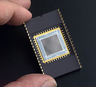
A charge-coupled device (CCD) is an integrated circuit containing an array of linked, or coupled, capacitors. Under the control of an external circuit, each capacitor can transfer its electric charge to a neighboring capacitor. CCD sensors are a major technology used in digital imaging.

<span class="mw-page-title-main">Photodiode</span> Converts light into current

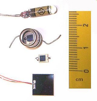
A photodiode is a semiconductor diode sensitive to photon radiation, such as visible light, infrared or ultraviolet radiation, X-rays and gamma rays. It produces an electrical current when it absorbs photons. This can be used for detection and measurement applications, or for the generation of electrical power in solar cells. Photodiodes are used in a wide range of applications throughout the electromagnetic spectrum from visible light photocells to gamma ray spectrometers.

<span class="mw-page-title-main">Digital camera</span> Camera that captures photographs or video in digital format

A digital camera, also called a digicam, is a camera that captures photographs in digital memory. Most cameras produced today are digital, largely replacing those that capture images on photographic film. Digital cameras are now widely incorporated into mobile devices like smartphones with the same or more capabilities and features of dedicated cameras. High-end, high-definition dedicated cameras are still commonly used by professionals and those who desire to take higher-quality photographs.

Digital image processing is the use of a digital computer to process digital images through an algorithm. As a subcategory or field of digital signal processing, digital image processing has many advantages over analog image processing. It allows a much wider range of algorithms to be applied to the input data and can avoid problems such as the build-up of noise and distortion during processing. Since images are defined over two dimensions digital image processing may be modeled in the form of multidimensional systems. The generation and development of digital image processing are mainly affected by three factors: first, the development of computers; second, the development of mathematics ; third, the demand for a wide range of applications in environment, agriculture, military, industry and medical science has increased.

<span class="mw-page-title-main">Sensor</span> Converter that measures a physical quantity and converts it into a signal

A sensor is a device that produces an output signal for the purpose of detecting a physical phenomenon.

Digital imaging or digital image acquisition is the creation of a digital representation of the visual characteristics of an object, such as a physical scene or the interior structure of an object. The term is often assumed to imply or include the processing, compression, storage, printing and display of such images. A key advantage of a digital image, versus an analog image such as a film photograph, is the ability to digitally propagate copies of the original subject indefinitely without any loss of image quality.

<span class="mw-page-title-main">Video camera</span> Camera used for electronic motion picture acquisition

A video camera is an optical instrument that captures videos, as opposed to a movie camera, which records images on film. Video cameras were initially developed for the television industry but have since become widely used for a variety of other purposes.

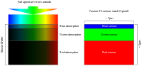
The Foveon X3 sensor is a digital camera image sensor designed by Foveon, Inc., and manufactured by Dongbu Electronics. It uses an array of photosites that consist of three vertically stacked photodiodes. Each of the three stacked photodiodes has a different spectral sensitivity, allowing it to respond differently to different wavelengths. The signals from the three photodiodes are then processed as additive color data that are transformed to a standard RGB color space.

A digital image is an image composed of picture elements, also known as pixels, each with finite, discrete quantities of numeric representation for its intensity or gray level that is an output from its two-dimensional functions fed as input by its spatial coordinates denoted with x, y on the x-axis and y-axis, respectively. Depending on whether the image resolution is fixed, it may be of vector or raster type. By itself, the term "digital image" usually refers to raster images or bitmapped images.

<span class="mw-page-title-main">Single-photon avalanche diode</span> Solid-state photodetector

A single-photon avalanche diode (SPAD), also called Geiger-mode avalanche photodiode is a solid-state photodetector within the same family as photodiodes and avalanche photodiodes (APDs), while also being fundamentally linked with basic diode behaviours. As with photodiodes and APDs, a SPAD is based around a semi-conductor p-n junction that can be illuminated with ionizing radiation such as gamma, x-rays, beta and alpha particles along with a wide portion of the electromagnetic spectrum from ultraviolet (UV) through the visible wavelengths and into the infrared (IR).

<span class="mw-page-title-main">Mixed-signal integrated circuit</span> Integrated circuit

A mixed-signal integrated circuit is any integrated circuit that has both analog circuits and digital circuits on a single semiconductor die. Their usage has grown dramatically with the increased use of cell phones, telecommunications, portable electronics, and automobiles with electronics and digital sensors.

<span class="mw-page-title-main">Photodetector</span> Sensors of light or other electromagnetic energy

Photodetectors, also called photosensors, are sensors of light or other electromagnetic radiation. There are a wide variety of photodetectors which may be classified by mechanism of detection, such as photoelectric or photochemical effects, or by various performance metrics, such as spectral response. Semiconductor-based photodetectors typically use a p–n junction that converts photons into charge. The absorbed photons make electron–hole pairs in the depletion region. Photodiodes and photo transistors are a few examples of photo detectors. Solar cells convert some of the light energy absorbed into electrical energy.

<span class="mw-page-title-main">Electronic component</span> Discrete device in an electronic system

An electronic component is any basic discrete electronic device or physical entity part of an electronic system used to affect electrons or their associated fields. Electronic components are mostly industrial products, available in a singular form and are not to be confused with electrical elements, which are conceptual abstractions representing idealized electronic components and elements. A datasheet for an electronic component is a technical document that provides detailed information about the component's specifications, characteristics, and performance.

A time delay and integration or time delay integration (TDI) charge-coupled device (CCD) is an image sensor for capturing images of moving objects at low light levels. While using similar underlying CCD technology, in operation it contrasts with staring arrays and line scanned arrays. It works by synchronized mechanical and electronical scanning, so that the effects of dim imaging targets on the sensor can be integrated over longer periods of time.

<span class="mw-page-title-main">History of the camera</span> Review of the topic

The history of the camera began even before the introduction of photography. Cameras evolved from the camera obscura through many generations of photographic technology – daguerreotypes, calotypes, dry plates, film – to the modern day with digital cameras and camera phones.

<span class="mw-page-title-main">Digital photography</span> Photography with a digital camera

Digital photography uses cameras containing arrays of electronic photodetectors interfaced to an analog-to-digital converter (ADC) to produce images focused by a lens, as opposed to an exposure on photographic film. The digitized image is stored as a computer file ready for further digital processing, viewing, electronic publishing, or digital printing. It is a form of digital imaging based on gathering visible light.

<span class="mw-page-title-main">Active-pixel sensor</span> Image sensor, consisting of an integrated circuit

An active-pixel sensor (APS) is an image sensor, which was invented by Peter J.W. Noble in 1968, where each pixel sensor unit cell has a photodetector and one or more active transistors. In a metal–oxide–semiconductor (MOS) active-pixel sensor, MOS field-effect transistors (MOSFETs) are used as amplifiers. There are different types of APS, including the early NMOS APS and the now much more common complementary MOS (CMOS) APS, also known as the CMOS sensor. CMOS sensors are used in digital camera technologies such as cell phone cameras, web cameras, most modern digital pocket cameras, most digital single-lens reflex cameras (DSLRs), mirrorless interchangeable-lens cameras (MILCs), and lensless imaging for cells.

<span class="mw-page-title-main">Color filter array</span>

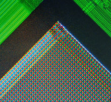
In digital imaging, a color filter array (CFA), or color filter mosaic (CFM), is a mosaic of tiny color filters placed over the pixel sensors of an image sensor to capture color information.

<span class="mw-page-title-main">Peter L. P. Dillon</span> American physicist

Peter L. P. Dillon is an American physicist, and the inventor of integral color image sensors.. and single-chip color video cameras. The curator of the Technology Collection at the George Eastman Museum, Todd Gustavson, has stated that "the color sensor technology developed by Peter Dillon has revolutionized all forms of color photography. These color sensors are now ubiquitous in products such as smart phone cameras, digital cameras and camcorders, digital cinema cameras, medical cameras, automobile cameras, and drones". Dillon joined Kodak Research Labs in 1959 and retired from Kodak in 1991. He lives in Pittsford, New York.

References

  1. 1 2 Lyon, Richard F. (August 1981). "The Optical Mouse, and an Architectural Methodology for Smart Digital Sensors" (PDF). In H. T. Kung; Robert F. Sproull; Guy L. Steele (eds.). VLSI Systems and Computations. Computer Science Press. pp. 1–19. doi:10.1007/978-3-642-68402-9_1. ISBN   978-3-642-68404-3. S2CID   60722329.
  2. 1 2 Lyon, Richard F. (2014). "The Optical Mouse: Early Biomimetic Embedded Vision". Advances in Embedded Computer Vision. Springer. pp. 3–22 (3). ISBN   9783319093871.
  3. Brain, Marshall; Carmack, Carmen (24 April 2000). "How Computer Mice Work". HowStuffWorks . Retrieved 9 October 2019.
  4. Cressler, John D. (2017). "Let There Be Light: The Bright World of Photonics". Silicon Earth: Introduction to Microelectronics and Nanotechnology, Second Edition. CRC Press. p. 29. ISBN   978-1-351-83020-1.
  5. Sze, Simon Min; Lee, Ming-Kwei (May 2012). "MOS Capacitor and MOSFET". Semiconductor Devices: Physics and Technology : International Student Version. John Wiley & Sons. ISBN   9780470537947 . Retrieved 6 October 2019.
  6. 1 2 3 4 Fossum, Eric R. (12 July 1993). Blouke, Morley M. (ed.). "Active pixel sensors: are CCDs dinosaurs?". SPIE Proceedings Vol. 1900: Charge-Coupled Devices and Solid State Optical Sensors III. Charge-Coupled Devices and Solid State Optical Sensors III. 1900. International Society for Optics and Photonics: 2–14. Bibcode:1993SPIE.1900....2F. CiteSeerX   10.1.1.408.6558 . doi:10.1117/12.148585. S2CID   10556755.
  7. 1 2 3 4 5 6 7 8 Fossum, Eric R.; Hondongwa, D. B. (2014). "A Review of the Pinned Photodiode for CCD and CMOS Image Sensors". IEEE Journal of the Electron Devices Society. 2 (3): 33–43. doi: 10.1109/JEDS.2014.2306412 .
  8. "CMOS Is Winning the Camera Sensor Battle, and Here's Why". techhive.com. 2011-12-29. Archived from the original on 2017-05-01. Retrieved 2017-04-27.
  9. 1 2 "CCD and CMOS sensors". Canon Professional Network. Archived from the original on 28 April 2018. Retrieved 28 April 2018.
  10. "What is a backlit CMOS sensor?". techradar.com. 2012-07-02. Archived from the original on 2017-05-06. Retrieved 2017-04-27.
  11. Moynihan, Tom (29 December 2011). "CMOS Is Winning the Camera Sensor Battle, and Here's Why". Archived from the original on 25 September 2015. Retrieved 10 April 2015.
  12. scmos.com Archived 2012-06-03 at the Wayback Machine , home page
  13. ieee.org - CCD in CMOS Archived 2015-06-22 at the Wayback Machine Padmakumar R. Rao et al., "CCD structures implemented in standard 0.18 μm CMOS technology"
  14. Nakamura, Junichi (2005). Image Sensors and Signal Processing for Digital Still Cameras. CRC Press. pp. 169–172. ISBN   9781420026856.
  15. Dillon, Peter (Dec 1976). "Integral color filter arrays for solid state imagers". 1976 International Electron Devices Meeting. pp. 400–403. doi:10.1109/IEDM.1976.189067. S2CID   35103154 via IEEE.{{cite book}}: |journal= ignored (help)
  16. Parulski, Kenneth (August 1985). "Color Filters and Processing Alternatives for One-chip Cameras". IEEE Transactions on Electron Devices. 32 (8): 1381–1389. Bibcode:1985ITED...32.1381P. doi:10.1109/T-ED.1985.22133. S2CID   9008653.
  17. Dillon, Peter (February 1978). "Fabrication and performance of color filter arrays for solid-state imagers". IEEE Transactions on Electron Devices. 25 (2): 97–101. Bibcode:1978ITED...25...97D. doi:10.1109/T-ED.1978.19045.
  18. Dillon, Peter (February 1978). "Color imaging system using a single CCD area array". IEEE Transactions on Electron Devices. 25 (2): 102–107. doi:10.1109/T-ED.1978.19046.
  19. "Deepest Ever Look into Orion". Archived from the original on 13 July 2016. Retrieved 13 July 2016.
  20. Gitto, Simone (2020). Arduino with MATLAB in the thermography: From the sensor to the thermal camera (Arduino and Beyond). Independently published. ISBN   979-8698999171.
  21. Dent, Steve (8 July 2014). "Sony's first 'curved sensor' photo may herald better images, cheaper lenses". Archived from the original on July 11, 2014. Retrieved July 8, 2014.
  22. Musburger, Robert B.; Ogden, Michael R. (2014). Single-Camera Video Production. CRC Press. p. 64. ISBN   9781136778445.
  23. 1 2 3 Williams, J. B. (2017). The Electronics Revolution: Inventing the Future. Springer. pp. 245–8. ISBN   9783319490885.
  24. 1 2 Ohta, Jun (2017). Smart CMOS Image Sensors and Applications. CRC Press. p. 2. ISBN   9781420019155.
  25. "1960: Metal Oxide Semiconductor (MOS) Transistor Demonstrated". The Silicon Engine. Computer History Museum . Retrieved August 31, 2019.
  26. Kozlowski, L. J.; Luo, J.; Kleinhans, W. E.; Liu, T. (14 September 1998). Pain, Bedabrata; Lomheim, Terrence S. (eds.). "Comparison of passive and active pixel schemes for CMOS visible imagers". Infrared Readout Electronics IV. 3360. International Society for Optics and Photonics: 101–110. Bibcode:1998SPIE.3360..101K. doi:10.1117/12.584474. S2CID   123351913.
  27. Daily Consular and Trade Reports. Department of Commerce and Labor, Bureau of Manufactures. 1914.
  28. Web, Desk (2022-06-25). "Samsung Electronics releases a sensor with 200 million pixels". BOL News. Retrieved 2022-06-25.
  29. Janesick, James R. (2001). Scientific charge-coupled devices. SPIE Press. pp. 3–4. ISBN   978-0-8194-3698-6.
  30. Boyle, William S; Smith, George E. (1970). "Charge Coupled Semiconductor Devices". Bell Syst. Tech. J. 49 (4): 587–593. Bibcode:1970BSTJ...49..587B. doi:10.1002/j.1538-7305.1970.tb01790.x.
  31. U.S. Patent 4,484,210: Solid-state imaging device having a reduced image lag
  32. Fossum, Eric R. (2007). "Active Pixel Sensors" (PDF). Semantic Scholar . S2CID   18831792. Archived from the original (PDF) on 9 March 2019. Retrieved 8 October 2019.
  33. Matsumoto, Kazuya; et al. (1985). "A new MOS phototransistor operating in a non-destructive readout mode". Japanese Journal of Applied Physics. 24 (5A): L323. Bibcode:1985JaJAP..24L.323M. doi:10.1143/JJAP.24.L323. S2CID   108450116.
  34. "CMOS Image Sensor Sales Stay on Record-Breaking Pace". IC Insights. May 8, 2018. Retrieved 6 October 2019.
  35. Benchoff, Brian (17 April 2016). "Building the First Digital Camera". Hackaday . Retrieved 30 April 2016. the Cyclops was the first digital camera
  36. Brain, Marshall; Carmack, Carmen (24 April 2000). "How Computer Mice Work". HowStuffWorks . Retrieved 9 October 2019.
  37. "Super Sensitive Sensor Sees What You Can't". npr.org. Archived from the original on 24 March 2018. Retrieved 28 April 2018.