
Chemical vapor deposition (CVD) is a vacuum deposition method used to produce high-quality, and high-performance, solid materials. The process is often used in the semiconductor industry to produce thin films.

MEMS is the technology of microscopic devices incorporating both electronic and moving parts. MEMS are made up of components between 1 and 100 micrometres in size, and MEMS devices generally range in size from 20 micrometres to a millimetre, although components arranged in arrays can be more than 1000 mm2. They usually consist of a central unit that processes data and several components that interact with the surroundings.
In semiconductor manufacturing plasma ashing is the process of removing the photoresist from an etched wafer. Using a plasma source, a monatomic substance known as a reactive species is generated. Oxygen or fluorine are the most common reactive species. Other gases used are N2/H2 where the H2 portion is 2%. The reactive species combines with the photoresist to form ash which is removed with a vacuum pump.
In physics, sputtering is a phenomenon in which microscopic particles of a solid material are ejected from its surface, after the material is itself bombarded by energetic particles of a plasma or gas. It occurs naturally in outer space, and can be an unwelcome source of wear in precision components. However, the fact that it can be made to act on extremely fine layers of material is utilised in science and industry—there, it is used to perform precise etching, carry out analytical techniques, and deposit thin film layers in the manufacture of optical coatings, semiconductor devices and nanotechnology products. It is a physical vapor deposition technique.
Reactive-ion etching (RIE) is an etching technology used in microfabrication. RIE is a type of dry etching which has different characteristics than wet etching. RIE uses chemically reactive plasma to remove material deposited on wafers. The plasma is generated under low pressure (vacuum) by an electromagnetic field. High-energy ions from the plasma attack the wafer surface and react with it.
An inductively coupled plasma (ICP) or transformer coupled plasma (TCP) is a type of plasma source in which the energy is supplied by electric currents which are produced by electromagnetic induction, that is, by time-varying magnetic fields.
Dry etching refers to the removal of material, typically a masked pattern of semiconductor material, by exposing the material to a bombardment of ions that dislodge portions of the material from the exposed surface. A common type of dry etching is reactive-ion etching. Unlike with many of the wet chemical etchants used in wet etching, the dry etching process typically etches directionally or anisotropically.
Surface micromachining builds microstructures by deposition and etching structural layers over a substrate. This is different from Bulk micromachining, in which a silicon substrate wafer is selectively etched to produce structures.
Bulk micromachining is a process used to produce micromachinery or microelectromechanical systems (MEMS).
Deep reactive-ion etching (DRIE) is a special subclass of reactive-ion etching (RIE). It enables highly anisotropic etch process used to create deep penetration, steep-sided holes and trenches in wafers/substrates, typically with high aspect ratios. It was developed for microelectromechanical systems (MEMS), which require these features, but is also used to excavate trenches for high-density capacitors for DRAM and more recently for creating through-silicon vias (TSVs) in advanced 3D wafer level packaging technology.

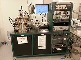
Microfabrication is the process of fabricating miniature structures of micrometre scales and smaller. Historically, the earliest microfabrication processes were used for integrated circuit fabrication, also known as "semiconductor manufacturing" or "semiconductor device fabrication". In the last two decades microelectromechanical systems (MEMS), microsystems, micromachines and their subfields, microfluidics/lab-on-a-chip, optical MEMS, RF MEMS, PowerMEMS, BioMEMS and their extension into nanoscale have re-used, adapted or extended microfabrication methods. Flat-panel displays and solar cells are also using similar techniques.
Plasma etching is a form of plasma processing used to fabricate integrated circuits. It involves a high-speed stream of glow discharge (plasma) of an appropriate gas mixture being shot at a sample. The plasma source, known as etch species, can be either charged (ions) or neutral. During the process, the plasma generates volatile etch products at room temperature from the chemical reactions between the elements of the material etched and the reactive species generated by the plasma. Eventually the atoms of the shot element embed themselves at or just below the surface of the target, thus modifying the physical properties of the target.

Xenon difluoride is a powerful fluorinating agent with the chemical formula XeF
2, and one of the most stable xenon compounds. Like most covalent inorganic fluorides it is moisture-sensitive. It decomposes on contact with water vapor, but is otherwise stable in storage. Xenon difluoride is a dense, colourless crystalline solid.

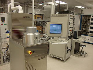
Lam Research Corporation is an American supplier of wafer-fabrication equipment and related services to the semiconductor industry. Its products are used primarily in front-end wafer processing, which involves the steps that create the active components of semiconductor devices and their wiring (interconnects). The company also builds equipment for back-end wafer-level packaging (WLP) and for related manufacturing markets such as for microelectromechanical systems (MEMS).

Plasma-enhanced chemical vapor deposition (PECVD) is a chemical vapor deposition process used to deposit thin films from a gas state (vapor) to a solid state on a substrate. Chemical reactions are involved in the process, which occur after creation of a plasma of the reacting gases. The plasma is generally created by radio frequency (RF) frequency or direct current (DC) discharge between two electrodes, the space between which is filled with the reacting gases.

Etching is used in microfabrication to chemically remove layers from the surface of a wafer during manufacturing. Etching is a critically important process module in fabrication, and every wafer undergoes many etching steps before it is complete.
Alcatel Micro Machining Systems (AMMS) was a French manufacturer of Deep Reactive Ion Etching systems. The company's headquarters were located in Annecy, France.
Plasma-activated bonding is a derivative, directed to lower processing temperatures for direct bonding with hydrophilic surfaces. The main requirements for lowering temperatures of direct bonding are the use of materials melting at low temperatures and with different coefficients of thermal expansion (CTE).

Low-energy plasma-enhanced chemical vapor deposition (LEPECVD) is a plasma-enhanced chemical vapor deposition technique used for the epitaxial deposition of thin semiconductor films. A remote low energy, high density DC argon plasma is employed to efficiently decompose the gas phase precursors while leaving the epitaxial layer undamaged, resulting in high quality epilayers and high deposition rates.
Vapor etching refers to a process used in the fabrication of Microelectromechanical systems (MEMS) and Nanoelectromechanical systems (NEMS). Sacrificial layers are isotropically etched using gaseous acids such as Hydrogen fluoride and Xenon difluoride to release the free standing components of the device.