
Semiconductor device fabrication is the process used to manufacture semiconductor devices, typically the metal–oxide–semiconductor (MOS) devices used in the integrated circuit (IC) chips such as modern computer processors, microcontrollers, and memory chips such as NAND flash and DRAM that are present in everyday electrical and electronic devices. It is a multiple-step sequence of photolithographic and chemical processing steps during which electronic circuits are gradually created on a wafer made of pure semiconducting material. Silicon is almost always used, but various compound semiconductors are used for specialized applications.
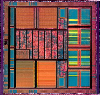
Very large-scale integration (VLSI) is the process of creating an integrated circuit (IC) by combining millions of MOS transistors onto a single chip. VLSI began in the 1970s when MOS integrated circuit chips were widely adopted, enabling complex semiconductor and telecommunication technologies to be developed. The microprocessor and memory chips are VLSI devices. Before the introduction of VLSI technology, most ICs had a limited set of functions they could perform. An electronic circuit might consist of a CPU, ROM, RAM and other glue logic. VLSI enables IC designers to add all of these into one chip.
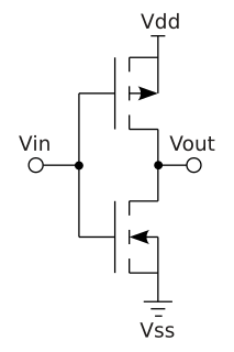
Complementary metal–oxide–semiconductor, also known as complementary-symmetry metal–oxide–semiconductor (COS-MOS), is a type of metal–oxide–semiconductor field-effect transistor (MOSFET) fabrication process that uses complementary and symmetrical pairs of p-type and n-type MOSFETs for logic functions. CMOS technology is used for constructing integrated circuit (IC) chips, including microprocessors, microcontrollers, memory chips, and other digital logic circuits. CMOS technology is also used for analog circuits such as image sensors, data converters, RF circuits, and highly integrated transceivers for many types of communication.

An application-specific integrated circuit is an integrated circuit (IC) chip customized for a particular use, rather than intended for general-purpose use. For example, a chip designed to run in a digital voice recorder or a high-efficiency video codec is an ASIC. Application-specific standard product (ASSP) chips are intermediate between ASICs and industry standard integrated circuits like the 7400 series or the 4000 series. ASIC chips are typically fabricated using metal-oxide-semiconductor (MOS) technology, as MOS integrated circuit chips.
In electronics and especially synchronous digital circuits, a clock signal oscillates between a high and a low state and is used like a metronome to coordinate actions of digital circuits.
Processor power dissipation or processing unit power dissipation is the process in which computer processors consume electrical energy, and dissipate this energy in the form of heat due to the resistance in the electronic circuits.
In digital circuit design, register-transfer level (RTL) is a design abstraction which models a synchronous digital circuit in terms of the flow of digital signals (data) between hardware registers, and the logical operations performed on those signals.
In computer engineering, a logic family is one of two related concepts:

In semiconductor design, standard cell methodology is a method of designing application-specific integrated circuits (ASICs) with mostly digital-logic features. Standard cell methodology is an example of design abstraction, whereby a low-level very-large-scale integration (VLSI) layout is encapsulated into an abstract logic representation.
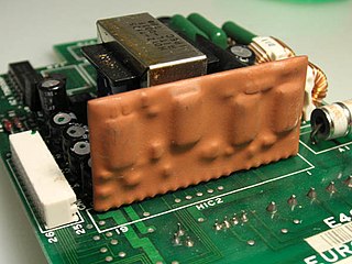
A hybrid integrated circuit (HIC), hybrid microcircuit, hybrid circuit or simply hybrid is a miniaturized electronic circuit constructed of individual devices, such as semiconductor devices and passive components, bonded to a substrate or printed circuit board (PCB). A PCB having components on a Printed Wiring Board (PWB) is not considered a true hybrid circuit according to the definition of MIL-PRF-38534.

Integrated circuit design, or IC design, is a sub-field of electronics engineering, encompassing the particular logic and circuit design techniques required to design integrated circuits, or ICs. ICs consist of miniaturized electronic components built into an electrical network on a monolithic semiconductor substrate by photolithography.

Signal integrity or SI is a set of measures of the quality of an electrical signal. In digital electronics, a stream of binary values is represented by a voltage waveform. However, digital signals are fundamentally analog in nature, and all signals are subject to effects such as noise, distortion, and loss. Over short distances and at low bit rates, a simple conductor can transmit this with sufficient fidelity. At high bit rates and over longer distances or through various mediums, various effects can degrade the electrical signal to the point where errors occur and the system or device fails. Signal integrity engineering is the task of analyzing and mitigating these effects. It is an important activity at all levels of electronics packaging and assembly, from internal connections of an integrated circuit (IC), through the package, the printed circuit board (PCB), the backplane, and inter-system connections. While there are some common themes at these various levels, there are also practical considerations, in particular the interconnect flight time versus the bit period, that cause substantial differences in the approach to signal integrity for on-chip connections versus chip-to-chip connections.

In the design of integrated circuits, power network design is the analysis and design of on-chip conductor networks that distribute electrical power on a chip. As in all engineering, this involves tradeoffs - the network must have adequate performance, be sufficiently reliable, but should not use more resources than required.
Multi-threshold CMOS (MTCMOS) is a variation of CMOS chip technology which has transistors with multiple threshold voltages (Vth) in order to optimize delay or power. The Vth of a MOSFET is the gate voltage where an inversion layer forms at the interface between the insulating layer (oxide) and the substrate (body) of the transistor. Low Vth devices switch faster, and are therefore useful on critical delay paths to minimize clock periods. The penalty is that low Vth devices have substantially higher static leakage power. High Vth devices are used on non-critical paths to reduce static leakage power without incurring a delay penalty. Typical high Vth devices reduce static leakage by 10 times compared with low Vth devices.

In integrated circuit design, physical design is a step in the standard design cycle which follows after the circuit design. At this step, circuit representations of the components of the design are converted into geometric representations of shapes which, when manufactured in the corresponding layers of materials, will ensure the required functioning of the components. This geometric representation is called integrated circuit layout. This step is usually split into several sub-steps, which include both design and verification and validation of the layout.
A three-dimensional integrated circuit is a MOS integrated circuit (IC) manufactured by stacking silicon wafers or dies and interconnecting them vertically using, for instance, through-silicon vias (TSVs) or Cu-Cu connections, so that they behave as a single device to achieve performance improvements at reduced power and smaller footprint than conventional two dimensional processes. The 3D IC is one of several 3D integration schemes that exploit the z-direction to achieve electrical performance benefits in microelectronics and nanoelectronics.
In integrated circuits, optical interconnects refers to any system of transmitting signals from one part of an integrated circuit to another using light. Optical interconnects have been the topic of study due to the high latency and power consumption incurred by conventional metal interconnects in transmitting electrical signals over long distances, such as in interconnects classed as global interconnects. The International Technology Roadmap for Semiconductors (ITRS) has highlighted interconnect scaling as a problem for the semiconductor industry.
Power gating is a technique used in integrated circuit design to reduce power consumption, by shutting off the current to blocks of the circuit that are not in use. In addition to reducing stand-by or leakage power, power gating has the benefit of enabling Iddq testing.
In semiconductor manufacturing, the International Roadmap for Devices and Systems defines the 5 nm process as the MOSFET technology node following the 7 nm node. In 2020, Samsung and TSMC entered volume production of 5 nm chips, manufactured for companies including Apple, Marvell, Huawei and Qualcomm.
In integrated circuits (ICs), interconnects are structures that connect two or more circuit elements together electrically. The design and layout of interconnects on an IC is vital to its proper function, performance, power efficiency, reliability, and fabrication yield. The material interconnects are made from depends on many factors. Chemical and mechanical compatibility with the semiconductor substrate and the dielectric between the levels of interconnect is necessary, otherwise barrier layers are needed. Suitability for fabrication is also required; some chemistries and processes prevent the integration of materials and unit processes into a larger technology (recipe) for IC fabrication. In fabrication, interconnects are formed during the back-end-of-line after the fabrication of the transistors on the substrate.