
Electroplating, also known as electrochemical deposition or electrodeposition, is a process for producing a metal coating on a solid substrate through the reduction of cations of that metal by means of a direct electric current. The part to be coated acts as the cathode of an electrolytic cell; the electrolyte is a solution of a salt of the metal to be coated; and the anode is usually either a block of that metal, or of some inert conductive material. The current is provided by an external power supply.

A printed circuit board is a medium used to connect electronic components to one another in a controlled manner. It takes the form of a laminated sandwich structure of conductive and insulating layers: each of the conductive layers is designed with an artwork pattern of traces, planes and other features etched from one or more sheet layers of copper laminated onto and/or between sheet layers of a non-conductive substrate. Electrical components may be fixed to conductive pads on the outer layers in the shape designed to accept the component's terminals, generally by means of soldering, to both electrically connect and mechanically fasten them to it. Another manufacturing process adds vias: plated-through holes that allow interconnections between layers.

Metalworking is the process of shaping and reshaping metals to create useful objects, parts, assemblies, and large scale structures. As a term it covers a wide and diverse range of processes, skills, and tools for producing objects on every scale: from huge ships, buildings, and bridges down to precise engine parts and delicate jewelry.

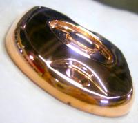
Chrome plating is a technique of electroplating a thin layer of chromium onto a metal object. A chrome plated part is called chrome, or is said to have been chromed. The chromium layer can be decorative, provide corrosion resistance, facilitate cleaning, or increase surface hardness. Sometimes, a less expensive substitute for chrome such as nickel may be used for aesthetic purposes.
Plating is a finishing process in which a metal is deposited on a surface. Plating has been done for hundreds of years; it is also critical for modern technology. Plating is used to decorate objects, for corrosion inhibition, to improve solderability, to harden, to improve wearability, to reduce friction, to improve paint adhesion, to alter conductivity, to improve IR reflectivity, for radiation shielding, and for other purposes. Jewelry typically uses plating to give a silver or gold finish.
Copper electroplating is the process of electroplating a layer of copper onto the surface of a metal object. Copper is used both as a standalone coating and as an undercoat onto which other metals are subsequently plated. The copper layer can be decorative, provide corrosion resistance, increase electrical and thermal conductivity, or improve the adhesion of additional deposits to the substrate.

Gold plating is a method of depositing a thin layer of gold onto the surface of another metal, most often copper or silver, by chemical or electrochemical plating. This article covers plating methods used in the modern electronics industry; for more traditional methods, often used for much larger objects, see gilding.

Metallizing is the general name for the technique of coating metal on the surface of objects. Metallic coatings may be decorative, protective or functional.
A via is an electrical connection between two or more metal layers, and are commonly used in printed circuit boards. Essentially a via is a small drilled hole that goes through two or more adjacent layers; the hole is plated with metal that forms an electrical connection through the insulating layers.

Electrotyping is a chemical method for forming metal parts that exactly reproduce a model. The method was invented by Moritz von Jacobi in Russia in 1838, and was immediately adopted for applications in printing and several other fields. As described in an 1890 treatise, electrotyping produces "an exact facsimile of any object having an irregular surface, whether it be an engraved steel- or copper-plate, a wood-cut, or a form of set-up type, to be used for printing; or a medal, medallion, statue, bust, or even a natural object, for art purposes."
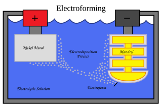
Electroforming is a metal forming process in which parts are fabricated through electrodeposition on a model, known in the industry as a mandrel. Conductive (metallic) mandrels are treated to create a mechanical parting layer, or are chemically passivated to limit electroform adhesion to the mandrel and thereby allow its subsequent separation. Non-conductive mandrels require the deposition of a conductive layer prior to electrodeposition. Such layers can be deposited chemically, or using vacuum deposition techniques. The outer surface of the mandrel forms the inner surface of the form.

Compact disc manufacturing is the process by which commercial compact discs (CDs) are replicated in mass quantities using a master version created from a source recording. This may be either in audio form (CD-DA) or data form (CD-ROM). This process is used in the mastering of read-only compact discs. DVDs and Blu-rays use similar methods.

Electroless deposition (ED) or electroless plating is defined as the autocatalytic process through which metals and metal alloys are deposited onto conductive and nonconductive surfaces. These nonconductive surfaces include plastics, ceramics, and glass etc., which can then become decorative, anti-corrosive, and conductive depending on their final functions. Electroplating unlike electroless deposition only deposits on other conductive or semi-conductive materials when a external current is applied. Electroless deposition deposits metals onto 2D and 3D structures such as screws, nanofibers, and carbon nanotubes, unlike other plating methods such as Physical Vapor Deposition ( PVD), Chemical Vapor Deposition (CVD), and electroplating, which are limited to 2D surfaces. Commonly the surface of the substrate is characterized via pXRD, SEM-EDS, and XPS which relay set parameters based their final funtionality. These parameters are referred to a Key Performance Indicators crucial for a researcher’ or company's purpose. Electroless deposition continues to rise in importance within the microelectronic industry, oil and gas, and aerospace industry.

LIGA is a fabrication technology used to create high-aspect-ratio microstructures. The term is a German acronym for Lithographie, Galvanoformung, Abformung – lithography, electroplating, and molding.

Cadmium oxide is an inorganic compound with the formula CdO. It is one of the main precursors to other cadmium compounds. It crystallizes in a cubic rocksalt lattice like sodium chloride, with octahedral cation and anion centers. It occurs naturally as the rare mineral monteponite. Cadmium oxide can be found as a colorless amorphous powder or as brown or red crystals. Cadmium oxide is an n-type semiconductor with a band gap of 2.18 eV at room temperature.

Electroless nickel-phosphorus plating, also referred to as E-nickel, is a chemical process that deposits an even layer of nickel-phosphorus alloy on the surface of a solid substrate, like metal or plastic. The process involves dipping the substrate in a water solution containing nickel salt and a phosphorus-containing reducing agent, usually a hypophosphite salt. It is the most common version of electroless nickel plating and is often referred by that name. A similar process uses a borohydride reducing agent, yielding a nickel-boron coating instead.
Mechanical plating, also known as peen plating, mechanical deposition, or impact plating, is a plating process that imparts the coating by cold welding fine metal particles to a workpiece. Mechanical galvanization is the same process, but applies to coatings that are thicker than 0.001 in (0.025 mm). It is commonly used to overcome hydrogen embrittlement problems. Commonly plated workpieces include nails, screws, nuts, washers, stampings, springs, clips, and sintered iron components.
Nickel electroplating is a technique of electroplating a thin layer of nickel onto a metal object. The nickel layer can be decorative, provide corrosion resistance, wear resistance, or used to build up worn or undersized parts for salvage purposes.

Galvanic corrosion is an electrochemical process in which one metal corrodes preferentially when it is in electrical contact with another, in the presence of an electrolyte. A similar galvanic reaction is exploited in primary cells to generate a useful electrical voltage to power portable devices. This phenomenon is named after Italian physician Luigi Galvani (1737-1798).
Electroless copper plating is a chemical process that deposits an even layer of copper on the surface of a solid substrate, like metal or plastic. The process involves dipping the substrate in a water solution containing copper salts and a reducing agent such as formaldehyde.
