
The Hall effect is the production of a potential difference across an electrical conductor that is transverse to an electric current in the conductor and to an applied magnetic field perpendicular to the current. It was discovered by Edwin Hall in 1879.
Spintronics, also known as spin electronics, is the study of the intrinsic spin of the electron and its associated magnetic moment, in addition to its fundamental electronic charge, in solid-state devices. The field of spintronics concerns spin-charge coupling in metallic systems; the analogous effects in insulators fall into the field of multiferroics.
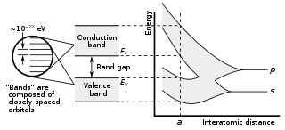
In solid-state physics and solid-state chemistry, a band gap, also called a bandgap or energy gap, is an energy range in a solid where no electronic states exist. In graphs of the electronic band structure of solids, the band gap refers to the energy difference between the top of the valence band and the bottom of the conduction band in insulators and semiconductors. It is the energy required to promote an electron from the valence band to the conduction band. The resulting conduction-band electron are free to move within the crystal lattice and serve as charge carriers to conduct electric current. It is closely related to the HOMO/LUMO gap in chemistry. If the valence band is completely full and the conduction band is completely empty, then electrons cannot move within the solid because there are no available states. If the electrons are not free to move within the crystal lattice, then there is no generated current due to no net charge carrier mobility. However, if some electrons transfer from the valence band to the conduction band, then current can flow. Therefore, the band gap is a major factor determining the electrical conductivity of a solid. Substances having large band gaps are generally insulators, those with small band gaps are semiconductor, and conductors either have very small band gaps or none, because the valence and conduction bands overlap to form a continuous band.

A semimetal is a material with a small energy overlap between the bottom of the conduction band and the top of the valence band, but they do not overlap in momentum space. According to electronic band theory, solids can be classified as insulators, semiconductors, semimetals, or metals. In insulators and semiconductors the filled valence band is separated from an empty conduction band by a band gap. For insulators, the magnitude of the band gap is larger than that of a semiconductor. Because of the slight overlap between the conduction and valence bands, semimetals have no band gap and a small density of states at the Fermi level. A metal, by contrast, has an appreciable density of states at the Fermi level because the conduction band is partially filled.

A high-electron-mobility transistor, also known as heterostructure FET (HFET) or modulation-doped FET (MODFET), is a field-effect transistor incorporating a junction between two materials with different band gaps as the channel instead of a doped region. A commonly used material combination is GaAs with AlGaAs, though there is wide variation, dependent on the application of the device. Devices incorporating more indium generally show better high-frequency performance, while in recent years, gallium nitride HEMTs have attracted attention due to their high-power performance.

In semiconductor production, doping is the intentional introduction of impurities into an intrinsic (undoped) semiconductor for the purpose of modulating its electrical, optical and structural properties. The doped material is referred to as an extrinsic semiconductor.
Organic semiconductors are solids whose building blocks are pi-bonded molecules or polymers made up by carbon and hydrogen atoms and – at times – heteroatoms such as nitrogen, sulfur and oxygen. They exist in the form of molecular crystals or amorphous thin films. In general, they are electrical insulators, but become semiconducting when charges are injected from appropriate electrodes or are introduced by doping or photoexcitation.

An organic field-effect transistor (OFET) is a field-effect transistor using an organic semiconductor in its channel. OFETs can be prepared either by vacuum evaporation of small molecules, by solution-casting of polymers or small molecules, or by mechanical transfer of a peeled single-crystalline organic layer onto a substrate. These devices have been developed to realize low-cost, large-area electronic products and biodegradable electronics. OFETs have been fabricated with various device geometries. The most commonly used device geometry is bottom gate with top drain and source electrodes, because this geometry is similar to the thin-film silicon transistor (TFT) using thermally grown SiO2 as gate dielectric. Organic polymers, such as poly(methyl-methacrylate) (PMMA), can also be used as dielectric. One of the benefits of OFETs, especially compared with inorganic TFTs, is their unprecedented physical flexibility, which leads to biocompatible applications, for instance in the future health care industry of personalized biomedicines and bioelectronics.
Magnetic semiconductors are semiconductor materials that exhibit both ferromagnetism and useful semiconductor properties. If implemented in devices, these materials could provide a new type of control of conduction. Whereas traditional electronics are based on control of charge carriers, practical magnetic semiconductors would also allow control of quantum spin state. This would theoretically provide near-total spin polarization, which is an important property for spintronics applications, e.g. spin transistors.
In particle physics, spin polarization is the degree to which the spin, i.e., the intrinsic angular momentum of elementary particles, is aligned with a given direction. This property may pertain to the spin, hence to the magnetic moment, of conduction electrons in ferromagnetic metals, such as iron, giving rise to spin-polarized currents. It may refer to (static) spin waves, preferential correlation of spin orientation with ordered lattices.

Mott insulators are a class of materials that are expected to conduct electricity according to conventional band theories, but turn out to be insulators. These insulators fail to be correctly described by band theories of solids due to their strong electron–electron interactions, which are not considered in conventional band theory. A Mott transition is a transition from a metal to an insulator, driven by the strong interactions between electrons. One of the simplest models that can capture Mott transition is the Hubbard model.

Spin-transfer torque (STT) is an effect in which the orientation of a magnetic layer in a magnetic tunnel junction or spin valve can be modified using a spin-polarized current.
The Rashba effect, also called Bychkov–Rashba effect, is a momentum-dependent splitting of spin bands in bulk crystals and low-dimensional condensed matter systems similar to the splitting of particles and anti-particles in the Dirac Hamiltonian. The splitting is a combined effect of spin–orbit interaction and asymmetry of the crystal potential, in particular in the direction perpendicular to the two-dimensional plane. This effect is named in honour of Emmanuel Rashba, who discovered it with Valentin I. Sheka in 1959 for three-dimensional systems and afterward with Yurii A. Bychkov in 1984 for two-dimensional systems.

The field-effect transistor (FET) is a type of transistor that uses an electric field to control the flow of current in a semiconductor. It comes in two types: junction FET (JFET) and metal-oxide-semiconductor FET (MOSFET). FETs have three terminals: source, gate, and drain. FETs control the flow of current by the application of a voltage to the gate, which in turn alters the conductivity between the drain and source.

Transition-metal dichalcogenide (TMD or TMDC) monolayers are atomically thin semiconductors of the type MX2, with M a transition-metal atom (Mo, W, etc.) and X a chalcogen atom (S, Se, or Te). One layer of M atoms is sandwiched between two layers of X atoms. They are part of the large family of so-called 2D materials, named so to emphasize their extraordinary thinness. For example, a MoS2 monolayer is only 6.5 Å thick. The key feature of these materials is the interaction of large atoms in the 2D structure as compared with first-row transition-metal dichalcogenides, e.g., WTe2 exhibits anomalous giant magnetoresistance and superconductivity.
Electric dipole spin resonance (EDSR) is a method to control the magnetic moments inside a material using quantum mechanical effects like the spin–orbit interaction. Mainly, EDSR allows to flip the orientation of the magnetic moments through the use of electromagnetic radiation at resonant frequencies. EDSR was first proposed by Emmanuel Rashba.
Spin gapless semiconductors are a novel class of materials with unique electrical band structure for different spin channels in such a way that there is no band gap for one spin channel while there is a finite gap in another spin channel.
Graphene is a semimetal whose conduction and valence bands meet at the Dirac points, which are six locations in momentum space, the vertices of its hexagonal Brillouin zone, divided into two non-equivalent sets of three points. The two sets are labeled K and K′. The sets give graphene a valley degeneracy of gv = 2. By contrast, for traditional semiconductors the primary point of interest is generally Γ, where momentum is zero. Four electronic properties separate it from other condensed matter systems.
Spin Hall magnetoresistance (SMR) is a transport phenomenon that is found in some electrical conductors that have at least one surface in direct contact with another magnetic material due to changes in the spin current that are present in metals and semiconductors with a large spin Hall angle. It is most easily detected when the magnetic material is an insulator which eliminates other magnetically sensitive transport effects arising from conduction in the magnetic material.

Spinterface is a term coined to indicate an interface between a ferromagnet and an organic semiconductor. This is a widely investigated topic in molecular spintronics, since the role of interfaces plays a huge part in the functioning of a device. In particular, spinterfaces are widely studied in the scientific community because of their hybrid organic/inorganic composition. In fact, the hybridization between the metal and the organic material can be controlled by acting on the molecules, which are more responsive to electrical and optical stimuli than metals. This gives rise to the possibility of efficiently tuning the magnetic properties of the interface at the atomic scale.
