The two inverters form a delay that holds the previous state of the bus and drives it back through a resistor.
A bus-holder or bus-keeper is a weak latch circuit that holds the last value on a tri-state bus.
The circuit is basically a delay element with the output connected back to the input through a relatively high impedance. This is usually achieved with two inverters connected in series, followed by a series resistor connected to the second inverter. The resistor drives the bus weakly; therefore other circuits can override the value of the bus when they are not in tri-state mode.
Bus-holders are used to prevent CMOS gate inputs from getting floating values when they are connected to tri-stated nets. Otherwise both transistors in the gate could get turned partially on, increasing power consumption and noise. In severe cases, this increased power consumption can destroy the CMOS gate. This is prevented by the bus-holder pulling the input to the last valid logic level (0 or 1) on the net. The circuit is usually placed in parallel with the tri-stated net.
A logic gate is a device that performs a Boolean function, a logical operation performed on one or more binary inputs that produces a single binary output. Depending on the context, the term may refer to an ideal logic gate, one that has, for instance, zero rise time and unlimited fan-out, or it may refer to a non-ideal physical device.
In electronics, a comparator is a device that compares two voltages or currents and outputs a digital signal indicating which is larger. It has two analog input terminals and and one binary digital output . The output is ideally
Transistor–transistor logic (TTL) is a logic family built from bipolar junction transistors. Its name signifies that transistors perform both the logic function and the amplifying function, as opposed to earlier resistor–transistor logic (RTL) and diode–transistor logic (DTL).
N-type metal–oxide–semiconductor logic uses n-type (-) MOSFETs to implement logic gates and other digital circuits. These nMOS transistors operate by creating an inversion layer in a p-type transistor body. This inversion layer, called the n-channel, can conduct electrons between n-type "source" and "drain" terminals. The n-channel is created by applying voltage to the third terminal, called the gate. Like other MOSFETs, nMOS transistors have four modes of operation: cut-off, triode, saturation, and velocity saturation.
In digital logic, an inverter or NOT gate is a logic gate which implements logical negation. It outputs a bit opposite of the bit that is put into it. The bits are typically implemented as two differing voltage levels.
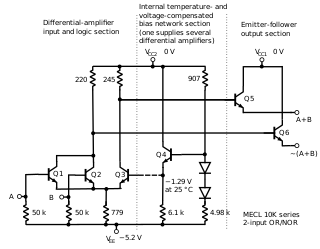
In electronics, emitter-coupled logic (ECL) is a high-speed integrated circuit bipolar transistor logic family. ECL uses an overdriven bipolar junction transistor (BJT) differential amplifier with single-ended input and limited emitter current to avoid the saturated region of operation and its slow turn-off behavior. As the current is steered between two legs of an emitter-coupled pair, ECL is sometimes called current-steering logic (CSL), current-mode logic (CML) or current-switch emitter-follower (CSEF) logic.
The 7400 series is a popular logic family of transistor–transistor logic (TTL) integrated circuits (ICs).
In electronics, a Schmitt trigger is a comparator circuit with hysteresis implemented by applying positive feedback to the noninverting input of a comparator or differential amplifier. It is an active circuit which converts an analog input signal to a digital output signal. The circuit is named a trigger because the output retains its value until the input changes sufficiently to trigger a change. In the non-inverting configuration, when the input is higher than a chosen threshold, the output is high. When the input is below a different (lower) chosen threshold the output is low, and when the input is between the two levels the output retains its value. This dual threshold action is called hysteresis and implies that the Schmitt trigger possesses memory and can act as a bistable multivibrator. There is a close relation between the two kinds of circuits: a Schmitt trigger can be converted into a latch and a latch can be converted into a Schmitt trigger.
Resistor–transistor logic (RTL), sometimes also known as transistor–resistor logic (TRL), is a class of digital circuits built using resistors as the input network and bipolar junction transistors (BJTs) as switching devices. RTL is the earliest class of transistorized digital logic circuit; it was succeeded by diode–transistor logic (DTL) and transistor–transistor logic (TTL).
In computer engineering, a logic family is one of two related concepts:
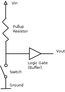
In electronic logic circuits, a pull-up resistor (PU) or pull-down resistor (PD) is a resistor used to ensure a known state for a signal. It is typically used in combination with components such as switches and transistors, which physically interrupt the connection of subsequent components to ground or to VCC. Closing the switch creates a direct connection to ground or VCC, but when the switch is open, the rest of the circuit would be left floating.
In digital electronics, a tri-state or three-state buffer is a type of digital buffer that has three stable states: a high output state, a low output state, and a high-impedance state. In the high-impedance state, the output of the buffer is disconnected from the output bus, allowing other devices to drive the bus without interference from the tri-state buffer. This can be useful in situations where multiple devices are connected to the same bus and need to take turns accessing it. Systems implementing three-state logic on their bus are known as a three-state bus or tri-state bus.
The NOR gate is a digital logic gate that implements logical NOR - it behaves according to the truth table to the right. A HIGH output (1) results if both the inputs to the gate are LOW (0); if one or both input is HIGH (1), a LOW output (0) results. NOR is the result of the negation of the OR operator. It can also in some senses be seen as the inverse of an AND gate. NOR is a functionally complete operation—NOR gates can be combined to generate any other logical function. It shares this property with the NAND gate. By contrast, the OR operator is monotonic as it can only change LOW to HIGH but not vice versa.
Diode logic constructs AND and OR logic gates with diodes and resistors.
Integrated injection logic (IIL, I2L, or I2L) is a class of digital circuits built with multiple collector bipolar junction transistors (BJT). When introduced it had speed comparable to TTL yet was almost as low power as CMOS, making it ideal for use in VLSI (and larger) integrated circuits. The gates can be made smaller with this logic family than with CMOS because complementary transistors are not needed. Although the logic voltage levels are very close (High: 0.7V, Low: 0.2V), I2L has high noise immunity because it operates by current instead of voltage. I2L was developed in 1971 by Siegfried K. Wiedmann and Horst H. Berger who originally called it merged-transistor logic (MTL). A disadvantage of this logic family is that the gates draw power when not switching unlike with CMOS.
Open collector, open drain, open emitter, and open source refer to integrated circuit (IC) output pin configurations that process the IC's internal function through a transistor with an exposed terminal that is internally unconnected. One of the IC's internal high or low voltage rails typically connects to another terminal of that transistor. When the transistor is off, the output is internally disconnected from any internal power rail, a state called "high-impedance" (Hi-Z). Open outputs configurations thus differ from push–pull outputs, which use a pair of transistors to output a specific voltage or current.
A flash ADC is a type of analog-to-digital converter that uses a linear voltage ladder with a comparator at each "rung" of the ladder to compare the input voltage to successive reference voltages. Often these reference ladders are constructed of many resistors; however, modern implementations show that capacitive voltage division is also possible. The output of these comparators is generally fed into a digital encoder, which converts the inputs into a binary value.
In digital circuits, a logic level is one of a finite number of states that a digital signal can inhabit. Logic levels are usually represented by the voltage difference between the signal and ground, although other standards exist. The range of voltage levels that represent each state depends on the logic family being used. A logic-level shifter can be used to allow compatibility between different circuits.
PMOS or pMOS logic is a family of digital circuits based on p-channel, enhancement mode metal–oxide–semiconductor field-effect transistors (MOSFETs). In the late 1960s and early 1970s, PMOS logic was the dominant semiconductor technology for large-scale integrated circuits before being superseded by NMOS and CMOS devices.
This page is based on this Wikipedia article Text is available under the CC BY-SA 4.0 license; additional terms may apply. Images, videos and audio are available under their respective licenses.