External links
- Website of ISO with details about ISO 20523 including list of content
- Webportal with basic information about the different types of carbon films
| Authority control databases: National |
|---|
Carbon films are thin film coatings which consist predominantly of the chemical element carbon. They include plasma polymer films, amorphous carbon films (diamond-like carbon, DLC), CVD diamond films as well as graphite films.
Carbon films are produced by deposition using gas-phase deposition processes, in most cases taking place in a vacuum: chemical vapor deposition, CVD or physical vapor deposition, PVD. They are deposited in the form of thin films with film thicknesses of just a few micrometres.
Carbon films make it possible to implement a large number of surface functions, especially in the field of tribology - in other words, in applications where wear is a major factor.
| Authority control databases: National |
|---|

Chemical vapor deposition (CVD) is a vacuum deposition method used to produce high-quality, and high-performance, solid materials. The process is often used in the semiconductor industry to produce thin films.
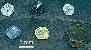
Lab-grown diamond is diamond that is produced in a controlled technological process. Unlike diamond simulants, synthetic diamonds are composed of the same material as naturally formed diamonds – pure carbon crystallized in an isotropic 3D form – and share identical chemical and physical properties.
CVD may refer to:
A thin film is a layer of material ranging from fractions of a nanometer (monolayer) to several micrometers in thickness. The controlled synthesis of materials as thin films is a fundamental step in many applications. A familiar example is the household mirror, which typically has a thin metal coating on the back of a sheet of glass to form a reflective interface. The process of silvering was once commonly used to produce mirrors, while more recently the metal layer is deposited using techniques such as sputtering. Advances in thin film deposition techniques during the 20th century have enabled a wide range of technological breakthroughs in areas such as magnetic recording media, electronic semiconductor devices, integrated passive devices, LEDs, optical coatings, hard coatings on cutting tools, and for both energy generation and storage. It is also being applied to pharmaceuticals, via thin-film drug delivery. A stack of thin films is called a multilayer.
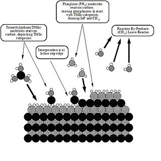
Metalorganic vapour-phase epitaxy (MOVPE), also known as organometallic vapour-phase epitaxy (OMVPE) or metalorganic chemical vapour deposition (MOCVD), is a chemical vapour deposition method used to produce single- or polycrystalline thin films. It is a process for growing crystalline layers to create complex semiconductor multilayer structures. In contrast to molecular-beam epitaxy (MBE), the growth of crystals is by chemical reaction and not physical deposition. This takes place not in vacuum, but from the gas phase at moderate pressures. As such, this technique is preferred for the formation of devices incorporating thermodynamically metastable alloys, and it has become a major process in the manufacture of optoelectronics, such as Light-emitting diodes. It was invented in 1968 at North American Aviation Science Center by Harold M. Manasevit.
On 8 September 2011 Nuon announced the pilot plant would be closed down since no investor for production expansion could be found. However, on 7 May 2012 Nuon announced that Helianthos has been sold to HyET Solar.
Electron-beam physical vapor deposition, or EBPVD, is a form of physical vapor deposition in which a target anode is bombarded with an electron beam given off by a charged tungsten filament under high vacuum. The electron beam causes atoms from the target to transform into the gaseous phase. These atoms then precipitate into solid form, coating everything in the vacuum chamber with a thin layer of the anode material.
Vacuum deposition is a group of processes used to deposit layers of material atom-by-atom or molecule-by-molecule on a solid surface. These processes operate at pressures well below atmospheric pressure. The deposited layers can range from a thickness of one atom up to millimeters, forming freestanding structures. Multiple layers of different materials can be used, for example to form optical coatings. The process can be qualified based on the vapor source; physical vapor deposition uses a liquid or solid source and chemical vapor deposition uses a chemical vapor.
Isobutylgermane (IBGe, Chemical formula: (CH3)2CHCH2GeH3, is an organogermanium compound. It is a colourless, volatile liquid that is used in MOVPE (Metalorganic Vapor Phase Epitaxy) as an alternative to germane. IBGe is used in the deposition of Ge films and Ge-containing thin semiconductor films such as SiGe in strained silicon application, and GeSbTe in NAND Flash applications.

Hybrid physical–chemical vapor deposition (HPCVD) is a thin-film deposition technique, that combines physical vapor deposition (PVD) with chemical vapor deposition (CVD).
ASM is a Dutch headquartered multinational corporation that specializes in the design, manufacturing, sales and service of semiconductor wafer processing equipment for the fabrication of semiconductor devices. ASM's products are used by semiconductor manufacturers in front-end wafer processing in their semiconductor fabrication plants. ASM’s technologies include atomic layer deposition, epitaxy, chemical vapor deposition and diffusion.
Combustion chemical vapor deposition (CCVD) is a chemical process by which thin-film coatings are deposited onto substrates in the open atmosphere.
Chemical vapor deposition of ruthenium is a method to deposit thin layers of ruthenium on substrates by Chemical vapor deposition (CVD).
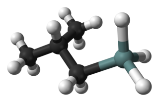
Trimethylsilane is the organosilicon compound with the formula (CH3)3SiH. It is a trialkylsilane. The Si-H bond is reactive. It is less commonly used as a reagent than the related triethylsilane, which is a liquid at room temperature.

Aerographite is a synthetic foam consisting of a porous interconnected network of tubular carbon. With a density of 180 g/m3 it is one of the lightest structural materials ever created. It was developed jointly by a team of researchers at the University of Kiel and the Technical University of Hamburg in Germany, and was first reported in a scientific journal in June 2012.
Karen Klincewicz Gleason is the Associate Provost at the Massachusetts Institute of Technology, where she has also served as the Alexander and I. Michael Kasser Professor of Chemical Engineering, from 2006–present. She has invented over 15 patented designs. She has developed a hydrophobic surface that can be applied in energy harvesting.
Nitrogen-doped carbon nanotubes (N-CNTs) can be produced through five main methods; chemical vapor deposition (CVD), high-temperature and high-pressure reactions, gas-solid reaction of amorphous carbon with NH3 at high temperature, solid reaction, and solvothermal synthesis.
Lisa McElwee-White is currently the Colonel Allen R. and Margaret G. Crow Professor of Chemistry at the University of Florida.
Laser chemical vapor deposition (LCVD) is a chemical process used to produce high purity, high performance films, fibers, and mechanical hardware (MEMS). It is a form of chemical vapor deposition in which a laser beam is used to locally heat the semiconductor substrate, causing the vapor deposition chemical reaction to proceed faster at that site. The process is used in the semiconductor industry for spot coating, the MEMS industry for 3-D printing of hardware such as springs and heating elements,2,6,7,9 and the composites industry for boron and ceramic fibers. As with conventional CVD, one or more gas phase precursors are thermally decomposed, and the resulting chemical species 1) deposit on a surface, or 2) react, form the desired compound, and then deposit on a surface, or a combination of (1) and (2).

Gilbert Daniel Nessim is a chemistry professor at Bar-Ilan University specializing in the synthesis of 1D and 2D nanomaterials for electronic, mechanic, and energy applications.