Related Research Articles
In integrated circuit manufacturing, photolithography or optical lithography is a general term used for techniques that use light to produce minutely patterned thin films of suitable materials over a substrate, such as a silicon wafer, to protect selected areas of it during subsequent etching, deposition, or implantation operations. Typically, ultraviolet light is used to transfer a geometric design from an optical mask to a light-sensitive chemical (photoresist) coated on the substrate. The photoresist either breaks down or hardens where it is exposed to light. The patterned film is then created by removing the softer parts of the coating with appropriate solvents, also known in this case as developers.

A photomask is an opaque plate with transparent areas that allow light to shine through in a defined pattern. Photomasks are commonly used in photolithography for the production of integrated circuits to produce a pattern on a thin wafer of material. Several masks are used in turn, each one reproducing a layer of the completed design, and together known as a mask set.
Naomi J. Halas is the Stanley C. Moore Professor in Electrical and Computer Engineering, and professor of biomedical engineering, chemistry and physics at Rice University. She is also the founding director of Rice University Laboratory for Nanophotonics, and the Smalley-Curl Institute. She invented the first nanoparticle with tunable plasmonic resonances, which are controlled by their shape and structure, and has won numerous awards for her pioneering work in the field of nanophotonics and plasmonics. She was also part of a team that developed the first dark pulse soliton in 1987 while working for IBM.
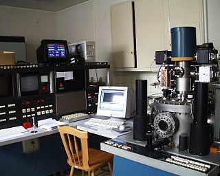
Electron-beam lithography is the practice of scanning a focused beam of electrons to draw custom shapes on a surface covered with an electron-sensitive film called a resist (exposing). The electron beam changes the solubility of the resist, enabling selective removal of either the exposed or non-exposed regions of the resist by immersing it in a solvent (developing). The purpose, as with photolithography, is to create very small structures in the resist that can subsequently be transferred to the substrate material, often by etching.
Nanolithography (NL) is a growing field of techniques within nanotechnology dealing with the engineering of nanometer-scale structures on various materials.
SPIE is an international not-for-profit professional society for optics and photonics technology, founded in 1955. It organizes technical conferences, trade exhibitions, and continuing education programs for researchers and developers in the light-based fields of physics, including: optics, photonics, and imaging engineering. The society publishes peer-reviewed scientific journals, conference proceedings, monographs, tutorial texts, field guides, and reference volumes in print and online. SPIE is especially well-known for Photonics West, one of the laser and photonics industry's largest combined conferences and tradeshows which is held annually in San Francisco. SPIE also participates as partners in leading educational initiatives, and in 2020, for example, provided more than $5.8 million in support of optics education and outreach programs around the world.
ASML Holding N.V. is a Dutch multinational corporation founded in 1984. ASML specializes in the development and manufacturing of photolithography machines which are used to produce computer chips.

Phase-shift masks are photomasks that take advantage of the interference generated by phase differences to improve image resolution in photolithography. There exist alternating and attenuated phase shift masks. A phase-shift mask relies on the fact that light passing through a transparent media will undergo a phase change as a function of its optical thickness.
KLA Corporation is an American capital equipment company based in Milpitas, California. It supplies process control and yield management systems for the semiconductor industry and other related nanoelectronics industries. The company's products and services are intended for all phases of wafer, reticle, integrated circuit (IC) and packaging production, from research and development to final volume manufacturing.

Optical proximity correction (OPC) is a photolithography enhancement technique commonly used to compensate for image errors due to diffraction or process effects. The need for OPC is seen mainly in the making of semiconductor devices and is due to the limitations of light to maintain the edge placement integrity of the original design, after processing, into the etched image on the silicon wafer. These projected images appear with irregularities such as line widths that are narrower or wider than designed, these are amenable to compensation by changing the pattern on the photomask used for imaging. Other distortions such as rounded corners are driven by the resolution of the optical imaging tool and are harder to compensate for. Such distortions, if not corrected for, may significantly alter the electrical properties of what was being fabricated. Optical proximity correction corrects these errors by moving edges or adding extra polygons to the pattern written on the photomask. This may be driven by pre-computed look-up tables based on width and spacing between features or by using compact models to dynamically simulate the final pattern and thereby drive the movement of edges, typically broken into sections, to find the best solution,. The objective is to reproduce the original layout drawn by the designer on the semiconductor wafer as well as possible.
Contact lithography, also known as contact printing, is a form of photolithography whereby the image to be printed is obtained by illumination of a photomask in direct contact with a substrate coated with an imaging photoresist layer.
Federico Capasso is an applied physicist and is one of the inventors of the quantum cascade laser during his work at Bell Laboratories. He is currently on the faculty of Harvard University.
PROLITH is a computer simulator modeling the optical and chemical aspects of photolithography. Chris Mack started developing PROLITH after he began working in the field of photolithography at the NSA in 1983.
Computational lithography is the set of mathematical and algorithmic approaches designed to improve the resolution attainable through photolithography. Computational lithography came to the forefront of photolithography technologies in 2008 when the semiconductor industry faced challenges associated with the transition to a 22 nanometer CMOS microfabrication process and has become instrumental in further shrinking the design nodes and topology of semiconductor transistor manufacturing.
The argon fluoride laser is a particular type of excimer laser, which is sometimes called an exciplex laser. With its 193-nanometer wavelength, it is a deep ultraviolet laser, which is commonly used in the production of semiconductor integrated circuits, eye surgery, micromachining, and scientific research. "Excimer" is short for "excited dimer", while "exciplex" is short for "excited complex". An excimer laser typically uses a mixture of a noble gas and a halogen gas, which under suitable conditions of electrical stimulation and high pressure, emits coherent stimulated radiation in the ultraviolet range.
Nanochannel glass materials are an experimental mask technology that is an alternate method for fabricating nanostructures, although optical lithography is the predominant patterning technique.

Kenneth L. Schroeder was an American technology-focused corporate executive. Schroeder served as CEO of KLA-Tencor, a supplier of process control and yield management products for the semiconductor and related microelectronics industries.
Peter Trefonas is a retired DuPont Fellow at DuPont, where he had worked on the development of electronic materials. He is known for innovations in the chemistry of photolithography, particularly the development of anti-reflective coatings and polymer photoresists that are used to create circuitry for computer chips. This work has supported the patterning of smaller features during the lithographic process, increasing miniaturization and microprocessor speed.
Edmund Y. Lam is a Chinese professor and associate dean of engineering at the University of Hong Kong.
Kevin Rolland Thompson was the Group Director, Research and Development/Optics at Synopsys, Inc. His work contributed to developments in nanolithography, astrophysics and the advancement of optics
References
- "Chris Mack joins tech advisory board of DFM startup". EE Times . September 14, 2005. Retrieved March 25, 2011.
- "SPIE Taps '09 Award Winners". Photonics.com. April 23, 2009. Retrieved March 25, 2011.
- "SPIE appoints Chris Mack editor of 'Journal of Micro/Nanolithography, MEMS, and MOEMS'". SPIE. February 17, 2011. Retrieved March 25, 2011.
- Mack, Chris (January 22, 2008). Fundamental Principles of Optical Lithography: The Science of Microfabrication. West Sussex, England: John Wiley & Sons. ISBN 978-0-470-72730-0.