
Microelectromechanical systems (MEMS), also written as micro-electro-mechanical systems and the related micromechatronics and microsystems constitute the technology of microscopic devices, particularly those with moving parts. They merge at the nanoscale into nanoelectromechanical systems (NEMS) and nanotechnology. MEMS are also referred to as micromachines in Japan and microsystem technology (MST) in Europe.
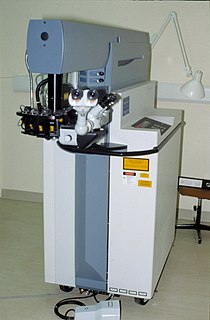
Photolithography, also called optical lithography or UV lithography, is a process used in microfabrication to pattern parts on a thin film or the bulk of a substrate. It uses light to transfer a geometric pattern from a photomask to a photosensitive chemical photoresist on the substrate. A series of chemical treatments then either etches the exposure pattern into the material or enables deposition of a new material in the desired pattern upon the material underneath the photoresist. In complex integrated circuits, a CMOS wafer may go through the photolithographic cycle as many as 50 times.

PARC is a research and development company in Palo Alto, California. Formed in 1969, the company was originally a subsidiary of Xerox, and was tasked with creating computer technology-related products and hardware systems.
An excimer laser, sometimes more correctly called an exciplex laser, is a form of ultraviolet laser which is commonly used in the production of microelectronic devices, semiconductor based integrated circuits or "chips", eye surgery, and micromachining.

A photomask is an opaque plate with holes or transparencies that allow light to shine through in a defined pattern. They are commonly used in photolithography and the production of integrated circuits in particular. Masks are used to produce a pattern on a substrate, normally a thin slice of silicon known as a wafer in the case of chip manufacturing. Several masks are used in turn, each one reproducing a layer of the completed design, and together they are known as a mask set.

Immersion lithography is a photolithography resolution enhancement technique for manufacturing integrated circuits (ICs) that replaces the usual air gap between the final lens and the wafer surface with a liquid medium that has a refractive index greater than one. The resolution is increased by a factor equal to the refractive index of the liquid. Current immersion lithography tools use highly purified water for this liquid, achieving feature sizes below 45 nanometers. ASML and Nikon are currently the only manufacturers of immersion lithography systems.
The 90 nm process refers to the level of MOSFET (CMOS) fabrication process technology that was commercialized by the 2003–2005 timeframe, by leading semiconductor companies like Toshiba, Sony, Samsung, IBM, Intel, Fujitsu, TSMC, Elpida, AMD, Infineon, Texas Instruments and Micron Technology.
Nanolithography is a growing field of techniques within nanotechnology dealing with the engineering of nanometer-scale structures. From Greek, the word can be broken up into three parts: "nano" meaning dwarf, "lith" meaning stone, and "graphy" meaning to write, or "tiny writing onto stone." Today, the word has evolved to cover the design of structures in the range of 10−9 to 10−6 meters, or structures in the nanometer range. Essentially, the field is a derivative of lithography, only covering significantly smaller structures. All nanolithographic techniques can be separated into two categories: those that etch away molecules leaving behind the desired structure, and those that directly write the desired structure to a surface.
Chris Mack is an expert in photolithography. He received multiple undergraduate degrees from Rose-Hulman Institute of Technology in 1982, a master of science degree in electrical engineering from the University of Maryland, College Park in 1989, and a PhD in chemical engineering from The University of Texas in 1998.
Next-generation lithography or NGL is a term used in integrated circuit manufacturing to describe the lithography technologies slated to replace open air, visible light photolithography. As of 2016 the most advanced form of photolithography was immersion lithography, in which water is used as an immersion medium for the final lens. It was applied to the 16 nm and 14 nm nodes, with the required use of multiple patterning. The increasing costs of multiple patterning have motivated the continued search for a next-generation technology that can flexibly achieve the required resolution in a single processing step.
ASML Holding N.V. is a Dutch company and currently the largest supplier in the world of photolithography systems for the semiconductor industry. The company manufactures machines for the production of integrated circuits. The company is a component of the Euro Stoxx 50 and NASDAQ-100.

Phase-shift masks are photomasks that take advantage of the interference generated by phase differences to improve image resolution in photolithography. There exist alternating and attenuated phase shift masks. A phase-shift mask relies on the fact that light passing through a transparent media will undergo a phase change as a function of its optical thickness.
The 32 nm node is the step following the 45 nm process in CMOS (MOSFET) semiconductor device fabrication. "32-nanometre" refers to the average half-pitch of a memory cell at this technology level. Toshiba produced commercial 32 GiB NAND flash memory chips with the 32 nm process in 2009. Intel and AMD produced commercial microchips using the 32-nanometre process in the early 2010s. IBM and the Common Platform also developed a 32 nm high-κ metal gate process. Intel began selling its first 32 nm processors using the Westmere architecture on 7 January 2010.

LIGA is a German acronym for Lithographie, Galvanoformung, Abformung that describes a fabrication technology used to create high-aspect-ratio microstructures.

Naval Surface Warfare Center Crane Division is the principal tenant command located at Naval Support Activity Crane. NSA Crane is a United States Navy installation located approximately 35 miles southwest of Bloomington, Indiana and predominantly located in Martin County, but small parts also extend into Greene and Lawrence counties. It was originally established in 1941 under the Bureau of Ordnance as the Naval Ammunition Depot for production, testing, and storage of ordnance under the first supplemental Defense Appropriation Act. The base is named after William M. Crane. The base is the third largest naval installation in the world by geographic area and employs approximately 3,300 people. The closest community is the small town of Crane, which lies adjacent to the northwest corner of the facility.
Computational lithography is the set of mathematical and algorithmic approaches designed to improve the resolution attainable through photolithography. Computational lithography has come to the forefront of photolithography in 2008 as the semiconductor industry grappled with the challenges associated with the transition to 22 nanometer CMOS process technology and beyond.

SÜSS MicroTec SE is a supplier of equipment and process solutions for the semiconductor industry and related markets. The microstructuring systems like photolithography tools are used for manufacturing of processors, memory chips, MEMS, LED and other micro system devices.
Nanochannel glass materials are an experimental mask technology that is an alternate method for fabricating nanostructures, although optical lithography is the predominant patterning technique.
Optica is an optical design program used for the design and analysis of both imaging and illumination systems. It works by ray tracing the propagation of rays through an optical system. It performs polarization ray-tracing, non-sequential ray-tracing, energy calculations, and optimization of optical systems in three-dimensional space. It also performs symbolic modeling of optical systems, diffraction, interference, wave-front, and Gaussian beam propagation calculations. In addition to conducting simulations of optical designs, Optica is used by scientists to create illustrations of the simulated results in publications. Some examples of Optica being used in simulations and illustrations include holography, x-ray optics, spectrometers, Cerenkov radiation, microwave optics, nonlinear optics, scattering, camera design,extreme ultraviolet lithography simulations, telescope optics, laser design, ultrashort pulse lasers, eye models, solar concentrators and Ring Imaging CHerenkov (RICH) particle detectors.
Peter Trefonas is a DuPont Fellow at DuPont, where he works on the development of electronic materials. He is known for innovations in the chemistry of photolithography, particularly the development of anti-reflective coatings and polymer photoresists that are used to create circuitry for computer chips. This work has supported the patterning of smaller features during the lithographic process, increasing miniaturization and microprocessor speed.