Cornell NanoScale Science and Technology Facility

Last updated

The Cornell NanoScale Science and Technology Facility (CNF) is a scientific user facility and cleanroom which is located at Cornell University in Ithaca, New York. The CNF is one of the sixteen members of the National Nanotechnology Coordinated Infrastructure (NNCI).

Cleanroom facility designed to maintain extremely low levels of particulates, such as dust, airborne organisms, or vaporized particles

A cleanroom or clean room is a laboratory facility ordinarily utilized as a part of specialized industrial production or scientific research, including the manufacture of pharmaceutical items and microprocessors. Cleanrooms are designed to maintain extremely low levels of particulates, such as dust, airborne organisms, or vaporized particles. Cleanrooms typically have a cleanliness level quantified by the number of particles per cubic meter at a predetermined molecule measure. The ambient outdoor air in a typical urban area contains 35,000,000 particles for each cubic meter in the size range 0.5 μm and bigger in measurement, equivalent to an ISO 9 cleanroom, while by comparison an ISO 1 cleanroom permits no particles in that size range and just 12 particles for each cubic meter of 0.3 μm and smaller.

Cornell University Private Ivy League research university in Upstate New York

Cornell University is a private and statutory Ivy League research university in Ithaca, New York. Founded in 1865 by Ezra Cornell and Andrew Dickson White, the university was intended to teach and make contributions in all fields of knowledge—from the classics to the sciences, and from the theoretical to the applied. These ideals, unconventional for the time, are captured in Cornell's founding principle, a popular 1868 Ezra Cornell quotation: "I would found an institution where any person can find instruction in any study."

Ithaca, New York City in New York, United States

Ithaca is a city in the Finger Lakes region of New York. It is the seat of Tompkins County, as well as the largest community in the Ithaca–Tompkins County metropolitan area. This area contains the municipalities of the Town of Ithaca, the village of Cayuga Heights, and other towns and villages in Tompkins County. The city of Ithaca is located on the southern shore of Cayuga Lake, in Central New York, about 45 miles (72 km) south-west of Syracuse. It is named after the Greek island of Ithaca. Additionally, Ithaca is located 247 miles (398 km) southeast of Toronto, and 223 miles (359 km) northwest of New York City.

The CNF was started as part of a National Science Foundation initiative in 1977, and has subsequently been partially supported by several other NSF programs. [1] It currently receives about $20 million each year in federal funding. [2] In 2004 the CNF moved into its current facility, Duffield Hall, supported by $100 million in support from Cornell. It now includes 15,000 square feet of Level 1000 cleanroom as well as several times more non-cleanroom laboratory space. [3] In 2009 the NNIN received $10 million as part of the American Recovery and Reinvestment Act. [4]

National Science Foundation United States government agency

The National Science Foundation (NSF) is a United States government agency that supports fundamental research and education in all the non-medical fields of science and engineering. Its medical counterpart is the National Institutes of Health. With an annual budget of about US$7.8 billion, the NSF funds approximately 24% of all federally supported basic research conducted by the United States' colleges and universities. In some fields, such as mathematics, computer science, economics, and the social sciences, the NSF is the major source of federal backing.

The CNF is a general user facility, and while many users are from Cornell or other nearby universities, it also draws users from a wide range of universities and companies around the world. [5] Roughly 700 scientists use the facility every year, half of whom are associated with Cornell. [6]

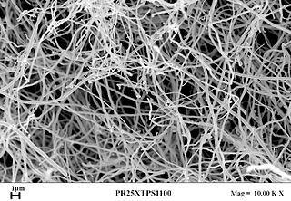
The CNF is used for research in a wide range of fields such as MEMS, microfluidics, nanomagnetics and bioelectronics. It includes fabrication tools for processes including electron-beam lithography, photolithography, chemical vapor deposition, electron-beam deposition and reactive ion etching. It also contains characterization equipment including scanning electron microscopes, ellipsometers and probe stations for electrical measurement.

Microfluidics deals with the behaviour, precise control and manipulation of fluids that are geometrically constrained to a small, typically sub-millimeter, scale at which capillary penetration governs mass transport. It is a multidisciplinary field at the intersection of engineering, physics, chemistry, biochemistry, nanotechnology, and biotechnology, with practical applications in the design of systems in which low volumes of fluids are processed to achieve multiplexing, automation, and high-throughput screening. Microfluidics emerged in the beginning of the 1980s and is used in the development of inkjet printheads, DNA chips, lab-on-a-chip technology, micro-propulsion, and micro-thermal technologies.

A nanomagnet is a submicrometric system that presents spontaneous magnetic order (magnetization) at zero applied magnetic field (remanence).

Bioelectronics is a field of research in the convergence of biology and electronics.

Related Research Articles

Microelectromechanical systems technology of very small devices

Microelectromechanical systems is the technology of microscopic devices, particularly those with moving parts. It merges at the nano-scale into nanoelectromechanical systems (NEMS) and nanotechnology. MEMS are also referred to as micromachines in Japan, or micro systems technology (MST) in Europe.

CNF may refer to:

SLAC National Accelerator Laboratory research center at Stanford University

SLAC National Accelerator Laboratory, originally named Stanford Linear Accelerator Center, is a United States Department of Energy National Laboratory operated by Stanford University under the programmatic direction of the U.S. Department of Energy Office of Science and located in Menlo Park, California.

Diamond Light Source UKs national synchrotron science facility located in Oxfordshire

Diamond Light Source is the UK's national synchrotron light source science facility located at the Harwell Science and Innovation Campus in Oxfordshire. Its purpose is to produce intense beams of light whose special characteristics are useful in many areas of scientific research. In particular it can be used to investigate the structure and properties of a wide range of materials from proteins, and engineering components to conservation of archeological artifacts.

The Center for Nanophase Materials Sciences(CNMS) was the first to open of the five Nanoscale Science Research Centers the United States Department of Energy sponsors. The Center's location is in Oak Ridge, Tennessee. The CNMS is a collaborative nanoscience user research facility for the synthesis, characterization, theory/ modeling/ simulation, and design of nanoscale materials and is co-located with Spallation Neutron Source.

Oxford Instruments United Kingdom manufacturing and research company

Oxford Instruments plc is a United Kingdom manufacturing and research company that designs and manufactures tools and systems for industry and research. The company is headquartered in Abingdon, Oxfordshire, England, with sites in the United Kingdom, United States, Europe, and Asia. It is listed on the London Stock Exchange and is a constituent of the FTSE 250 Index.

ISIS neutron source

ISIS Neutron and Muon Source is a pulsed neutron and muon source. It is situated at the Rutherford Appleton Laboratory of the Science and Technology Facilities Council, on the Harwell Science and Innovation Campus in Oxfordshire, United Kingdom. It uses the techniques of muon spectroscopy and neutron scattering to probe the structure and dynamics of condensed matter on a microscopic scale ranging from the subatomic to the macromolecular.

Focused ion beam

Focused ion beam, also known as FIB, is a technique used particularly in the semiconductor industry, materials science and increasingly in the biological field for site-specific analysis, deposition, and ablation of materials. A FIB setup is a scientific instrument that resembles a scanning electron microscope (SEM). However, while the SEM uses a focused beam of electrons to image the sample in the chamber, a FIB setup uses a focused beam of ions instead. FIB can also be incorporated in a system with both electron and ion beam columns, allowing the same feature to be investigated using either of the beams. FIB should not be confused with using a beam of focused ions for direct write lithography. These are generally quite different systems where the material is modified by other mechanisms.

Microfabrication processes of fabrication of miniature structures

Microfabrication is the process of fabricating miniature structures of micrometre scales and smaller. Historically, the earliest microfabrication processes were used for integrated circuit fabrication, also known as "semiconductor manufacturing" or "semiconductor device fabrication". In the last two decades microelectromechanical systems (MEMS), microsystems, micromachines and their subfields, microfluidics/lab-on-a-chip, optical MEMS, RF MEMS, PowerMEMS, BioMEMS and their extension into nanoscale have re-used, adapted or extended microfabrication methods. Flat-panel displays and solar cells are also using similar techniques.

Carbon nanofiber

Carbon nanofibers (CNFs), vapor grown carbon fibers (VGCFs), or vapor grown carbon nanofibers (VGCNFs) are cylindrical nanostructures with graphene layers arranged as stacked cones, cups or plates. Carbon nanofibers with graphene layers wrapped into perfect cylinders are called carbon nanotubes.

Advanced Light Source

The Advanced Light Source (ALS) is a research facility at Lawrence Berkeley National Laboratory in Berkeley, California. One of the world's brightest sources of ultraviolet and soft x-ray light, the ALS is the first "third-generation" synchrotron light source in its energy range, providing multiple extremely bright sources of intense and coherent short-wavelength light for use in scientific experiments by researchers from around the world. It is funded by the US Department of Energy (DOE) and operated by the University of California. In June 2018, Stephen Kevan became the director of the ALS.

Nanomanufacturing is both the production of nanoscaled materials, which can be powders or fluids, and the manufacturing of parts "bottom up" from nanoscaled materials or "top down" in smallest steps for high precision, used in several technologies such as laser ablation, etching and others. Nanomanufacturing differs from molecular manufacturing, which is the manufacture of complex, nanoscale structures by means of nonbiological mechanosynthesis.

Gas Cluster Ion Beams (GCIB) is a technology for nano-scale modification of surfaces. It can smooth a wide variety of surface material types to within an angstrom of roughness without subsurface damage. It is also used to chemically alter surfaces through infusion or deposition.

Electron-beam-induced deposition (EBID) is a process of decomposing gaseous molecules by an electron beam leading to deposition of non-volatile fragments onto a nearby substrate. The electron beam is usually provided by a scanning electron microscope, which results in high spatial accuracy and the possibility to produce free-standing, three-dimensional structures.

National Institute for Materials Science research institute in Japan

National Institute for Materials Science is an Independent Administrative Institution and one of the largest scientific research centers in Japan.

The Waterloo Institute for Nanotechnology (WIN) is located at the University of Waterloo and is co-located with the Institute for Quantum Computing in the Mike and Ophelia Lazaridis Quantum-Nano Centre (QNC). WIN is currently headed by Dr. Sushanta Mitra. Its inaugural director was Arthur Carty.

SUNY Poly Colleges of Nanoscale Science and Engineering

The Colleges of Nanoscale Science and Engineering are the colleges of nanotechnology at the SUNY Polytechnic Institute campus in Albany, New York. Founded in 2004 and formerly a component of the University at Albany, the colleges underwent rapid expansion in the late-2000s and early-2010s before merging with the SUNY Institute of Technology in 2014. As two of five colleges within SUNY Poly, they are the first colleges in the United States devoted to nanotechnology.

Environmental Molecular Sciences Laboratory

EMSL, or the William R. Wiley Environmental Molecular Sciences Laboratory, is a national scientific user facility located at Pacific Northwest National Laboratory in Richland, Washington. EMSL is funded by the Department of Energy’s Office of Biological and Environmental Research. EMSL provides experimental and computational resources to address the environmental molecular science challenges facing DOE and the nation.

Tokyo Electron Japanese company

Tokyo Electron Limited, or TEL, is a Japanese electronics and semiconductor company headquartered in Akasaka, Minato-ku, Tokyo, Japan.

Nano manufacturing is both the production of nanoscaled materials, which can be powders or fluids, and the manufacturing of parts "bottom up" from nanoscaled materials or "top down" in smallest steps for high precision, used in several technologies such as laser ablation, etching and others. Nanomanufacturing differs from molecular manufacturing, which is the manufacture of complex, nanoscale structures by means of nonbiological mechanosynthesis.

References

  1. "A Brief History of the CNF" . Retrieved May 16, 2012.
  2. "President's visit puts focus on upstate's high-tech growth" . Retrieved May 16, 2012.
  3. "Cornell NanoScale Science & Technology Facility" . Retrieved May 16, 2012.
  4. "Cornell NanoScale Science and Technology Facility Receives Stimulus Funds to Help with Equipment Upgrades". October 27, 2009. Retrieved May 16, 2012.
  5. "The 2010-2011 CNF Recearch Accomplishments" (PDF). Retrieved May 16, 2012.
  6. "Cornell NanoScale Science & Technology Facility (CNF) - Profile". Archived from the original on January 16, 2014. Retrieved May 16, 2012.