Furnace anneal

Last updated
External image
Searchtool.svg Anneal furnace, 2018

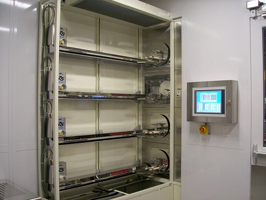
Furnace annealing is a process used in semiconductor device fabrication which consist of heating multiple semiconductor wafers in order to affect their electrical properties. Heat treatments are designed for different effects. Wafers can be heated in order to activate dopants, change film to film or film to wafer substrate interfaces, densify deposited films, change states of grown films, repair damage from implants, move dopants or drive dopants from one film into another or from a film into the wafer substrate. During ion implantation process, the crystal substrate is damaged due to bombardment with high energy ions. The damage caused can be repaired by subjecting the crystal to high temperature. This process is called annealing. Furnace anneals may be integrated into other furnace processing steps, such as oxidations, or may be processed on their own.

Furnace anneals are performed by equipment especially built to heat semiconductor wafers. Furnaces are capable of processing many wafers at a time but each process can last between several hours and a day. Increasingly, furnace anneals are being supplanted by Rapid Thermal Anneal (RTA) or Rapid Thermal Processing (RTP). This is due to the relatively long thermal cycles of furnaces that causes the dopants that are being activated, especially boron, to diffuse farther than is intended. RTP or RTA fixes this by having thermal cycles for each wafer that is of the order of minutes rather than hours for furnace anneals.

Equipment


Related Research Articles

Chemical vapor deposition Method used to make thin films for semiconductors or surface coating

Chemical vapor deposition (CVD) is a vacuum deposition method used to produce high quality, and high-performance, solid materials. The process is often used in the semiconductor industry to produce thin films.

Ion implantation Use of ions to cause chemical changes

Ion implantation is a low-temperature process by which ions of one element are accelerated into a solid target, thereby changing the physical, chemical, or electrical properties of the target. Ion implantation is used in semiconductor device fabrication and in metal finishing, as well as in materials science research. The ions can alter the elemental composition of the target if they stop and remain in the target. Ion implantation also causes chemical and physical changes when the ions impinge on the target at high energy. The crystal structure of the target can be damaged or even destroyed by the energetic collision cascades, and ions of sufficiently high energy can cause nuclear transmutation.

Microelectromechanical systems Very small devices that incorporate moving components

Microelectromechanical systems (MEMS), also written as micro-electro-mechanical systems and the related micromechatronics and microsystems constitute the technology of microscopic devices, particularly those with moving parts. They merge at the nanoscale into nanoelectromechanical systems (NEMS) and nanotechnology. MEMS are also referred to as micromachines in Japan and microsystem technology (MST) in Europe.

Semiconductor device fabrication Manufacturing process used to create integrated circuits

Semiconductor device fabrication is the process used to manufacture semiconductor devices, typically the metal–oxide–semiconductor (MOS) devices used in the integrated circuit (IC) chips such as modern computer processors, microcontrollers, and memory chips such as NAND flash and DRAM that are present in everyday electrical and electronic devices. It is a multiple-step sequence of photolithographic and chemical processing steps during which electronic circuits are gradually created on a wafer made of pure semiconducting material. Silicon is almost always used, but various compound semiconductors are used for specialized applications.

A semiconductor material has an electrical conductivity value falling between that of a conductor, such as metallic copper, and an insulator, such as glass. Its resistivity falls as its temperature rises; metals behave in the opposite way. Its conducting properties may be altered in useful ways by introducing impurities ("doping") into the crystal structure. When two differently doped regions exist in the same crystal, a semiconductor junction is created. The behavior of charge carriers, which include electrons, ions, and electron holes, at these junctions is the basis of diodes, transistors, and most modern electronics. Some examples of semiconductors are silicon, germanium, gallium arsenide, and elements near the so-called "metalloid staircase" on the periodic table. After silicon, gallium arsenide is the second-most common semiconductor and is used in laser diodes, solar cells, microwave-frequency integrated circuits, and others. Silicon is a critical element for fabricating most electronic circuits.

Heat treating Process of heating something to alter it

Heat treating is a group of industrial, thermal and metalworking processes used to alter the physical, and sometimes chemical, properties of a material. The most common application is metallurgical. Heat treatments are also used in the manufacture of many other materials, such as glass. Heat treatment involves the use of heating or chilling, normally to extreme temperatures, to achieve the desired result such as hardening or softening of a material. Heat treatment techniques include annealing, case hardening, precipitation strengthening, tempering, carburizing, normalizing and quenching. Although the term heat treatment applies only to processes where the heating and cooling are done for the specific purpose of altering properties intentionally, heating and cooling often occur incidentally during other manufacturing processes such as hot forming or welding.

Epitaxy Crystal growth process relative to the substrate

Epitaxy refers to a type of crystal growth or material deposition in which new crystalline layers are formed with one or more well-defined orientations with respect to the crystalline seed layer. The deposited crystalline film is called an epitaxial film or epitaxial layer. The relative orientation(s) of the epitaxial layer to the seed layer is defined in terms of the orientation of the crystal lattice of each material. For most epitaxial growths, the new layer is usually crystalline and each crystallographic domain of the overlayer must have a well-defined orientation relative to the substrate crystal structure. Epitaxy can involve single-crystal structures, although grain-to-grain epitaxy has been observed in granular films. For most technological applications, single domain epitaxy, which is the growth of an overlayer crystal with one well-defined orientation with respect to the substrate crystal, is preferred. Epitaxy can also play an important role while growing superlattice structures.

In semiconductor production, doping is the intentional introduction of impurities into an intrinsic semiconductor for the purpose of modulating its electrical, optical and structural properties. The doped material is referred to as an extrinsic semiconductor.

Rapid thermal processing (RTP) is a semiconductor manufacturing process which heats silicon wafers to temperatures exceeding 1,000°C for not more than a few seconds. During cooling wafer temperatures must be brought down slowly to prevent dislocations and wafer breakage due to thermal shock. Such rapid heating rates are often attained by high intensity lamps or lasers. These processes are used for a wide variety of applications in semiconductor manufacturing including dopant activation, thermal oxidation, metal reflow and chemical vapor deposition. Precise control of temperature profile and rapid ramp-up and ramp-down rates demanded by a RTP system cannot be achieved with conventional control strategies due to nonlinear and multi time-scale effects. Reinforcement Learning (RL) control strategies have been shown to offer superior performance compared to conventional control techniques.

In metallurgy and materials science, annealing is a heat treatment that alters the physical and sometimes chemical properties of a material to increase its ductility and reduce its hardness, making it more workable. It involves heating a material above its recrystallization temperature, maintaining a suitable temperature for an appropriate amount of time and then cooling.

Vacuum furnace

A vacuum furnace is a type of furnace in which the product in the furnace is surrounded by a vacuum during processing. The absence of air or other gases prevents oxidation, heat loss from the product through convection, and removes a source of contamination. This enables the furnace to heat materials to temperatures as high as 3,000 °C (5,432 °F) with select materials. Maximum furnace temperatures and vacuum levels depend on melting points and vapor pressures of heated materials. Vacuum furnaces are used to carry out processes such as annealing, brazing, sintering and heat treatment with high consistency and low contamination.

Thermal oxidation Process creating a thin layer of (usually) silicon dioxide

In microfabrication, thermal oxidation is a way to produce a thin layer of oxide on the surface of a wafer. The technique forces an oxidizing agent to diffuse into the wafer at high temperature and react with it. The rate of oxide growth is often predicted by the Deal–Grove model. Thermal oxidation may be applied to different materials, but most commonly involves the oxidation of silicon substrates to produce silicon dioxide.

Metal gate

A metal gate, in the context of a lateral metal–oxide–semiconductor (MOS) stack, is the gate electrode separated by an oxide from the transistor's channel – the gate material is made from a metal. In most MOS transistors since about the mid 1970s, the "M" for metal has been replaced by a non-metal gate material.

Plasma-immersion ion implantation

Plasma-immersion ion implantation (PIII) or pulsed-plasma doping is a surface modification technique of extracting the accelerated ions from the plasma by applying a high voltage pulsed DC or pure DC power supply and targeting them into a suitable substrate or electrode with a semiconductor wafer placed over it, so as to implant it with suitable dopants. The electrode is a cathode for an electropositive plasma, while it is an anode for an electronegative plasma. Plasma can be generated in a suitably designed vacuum chamber with the help of various plasma sources such as electron cyclotron resonance plasma source which yields plasma with the highest ion density and lowest contamination level, helicon plasma source, capacitively coupled plasma source, inductively coupled plasma source, DC glow discharge and metal vapor arc. The vacuum chamber can be of two types - diode and triode type depending upon whether the power supply is applied to the substrate as in the former case or to the perforated grid as in the latter.

ASM International Dutch ininformation technology company

ASM International is a Dutch headquartered multinational corporation that specializes in design, manufacturing, sales and service of semiconductor wafer processing equipment for the fabrication of semiconductor devices. ASM's products are used by semiconductor manufacturers in front-end wafer processing in their semiconductor fabrication plants. ASM’s technologies include atomic layer deposition, epitaxy, chemical vapor deposition and diffusion.

A dopant, also called a doping agent, is a trace of impurity element that is introduced into a chemical material to alter its original electrical or optical properties. The amount of dopant necessary to cause changes is typically very low. When doped into crystalline substances, the dopant's atoms get incorporated into its crystal lattice. The crystalline materials are frequently either crystals of a semiconductor such as silicon and germanium for use in solid-state electronics, or transparent crystals for use in the production of various laser types; however, in some cases of the latter, noncrystalline substances such as glass can also be doped with impurities.

Monolayer doping (MLD) in semiconductor production is a well controlled, wafer-scale surface doping technique first developed at the University of California, Berkeley, in 2007. This work is aimed for attaining controlled doping of semiconductor materials with atomic accuracy, especially at nanoscale, which is not easily obtained by other existing technologies. This technique is currently used for fabricating ultrashallow junctions (USJs) as the heavily doped source/drain (S/D) contacts of metal-oxide-semiconductor field effect transistors (MOSFETs) as well as enabling dopant profiling of nanostructures.

Ultra-high-purity steam, also called the clean steam, UHP steam or high purity water vapor, is used in a variety of industrial manufacturing processes that require oxidation or annealing. These processes include the growth of oxide layers on silicon wafers for the semiconductor industry, originally described by the Deal-Grove model, and for the formation of passivation layers used to improve the light capture ability of crystalline photovoltaic cells. Several methods and technologies can be employed to generate ultra high purity steam, including pyrolysis, bubbling, direct liquid injection and purified steam generation. The level of purity, or the relative lack of contamination, affects the quality of the oxide layer or annealed surface. The method of delivery affects growth rate, uniformity and electrical performance. Oxidation and annealing are common steps in the manufacture of such devices as microelectronics and solar cells.

Dopant Activation is the process of obtaining the desired electronic contribution from impurity species in a semiconductor host. The term is often restricted to the application of thermal energy following the ion implantation of dopants. In the most common industrial example, rapid thermal processing is applied to silicon following the ion implantation of dopants such as phosphorus, arsenic and boron. Vacancies generated at elevated temperature (1200 °C) facilitate the movement of these species from interstitial to substitutional lattice sites while amorphization damage from the implantation process recrystallizes. A relatively rapid process, peak temperature is often maintained for less than one second to minimize unwanted chemical diffusion.

James W. Mayer was an applied physicist, who was active in the field of ion-solid interactions. His accomplishments played a critical role in the development of the solid-state particle detector; the field of ion beam analysis of materials, and the application of ion implantation to semiconductors.